4 - 4
Description
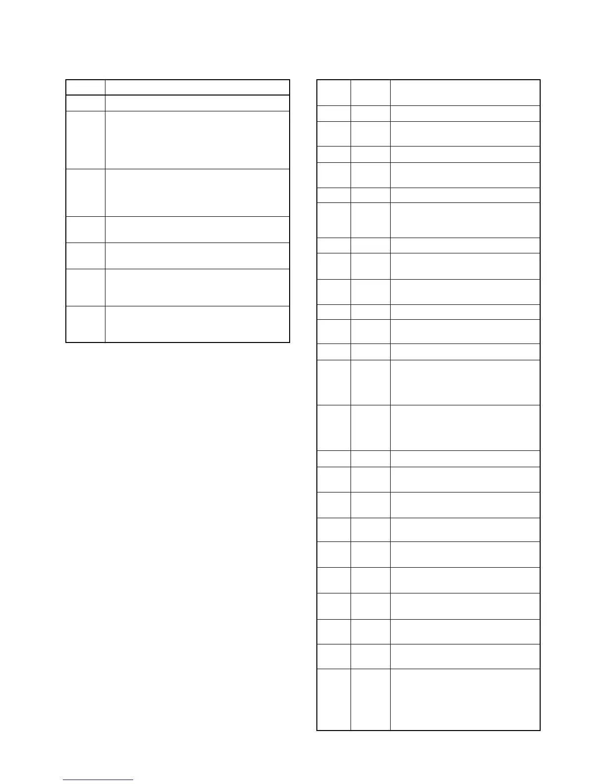
The voltage from a DC power supply.
The same voltage as the HV line which is con-
trolled by the power switching circuit (Q23, Q24).
When the [POWER] switch is pushed, the CPU
outputs the “PWON” control signal to the power
switching circuit to turn the circuit ON.
Common 5 V for the CPU converted from the HV
line by the CPU5V regulator circuit (IC10). The
circuit outputs the voltage regardless of the
power ON/OFF condition.
Common 8 V converted from the VCC line by the
8V regulator circuit (IC9).
Common 5 V converted from the 8 V and CPU5
lines by the 5V regulator circuit (Q27, Q28).
Receive 8 V controlled by the R8 regulator circuit
(Q26, Q30) using the “RXC” signal from the
expander IC (IC17, pin 4).
Transmit 8 V controlled by the T8 regulator circuit
(Q25, Q29, D23) using the “TMUT” signal from
the expander IC (IC17, pin 13).
Line
HV
VCC
CPU5V
8V
5V
R8V
T8V
Input port for the internal temperature.
Input port for the low voltage detection
from the connected power supply.
Input port for reset signal.
Output ports for 5/2 tone and DTMF
signals.
Outputs the CPU clock shift signal.
Outputs cut-off frequency control signal
to the low-pass filter (MAIN unit; IC5)
for CTCSS/DTCS switching.
Input port for the key matrix.
Output ports for 5/2 tone and DTMF
signals.
Input port for the PLL unlock signal
from the PLL IC (MAIN unit; IC4).
Input port for the key matrix.
Output ports for CTCSS/DTCS signals.
Input ports for the key matrix.
Outputs the clock signal to the PLL IC
(MAIN unit; IC4), D/A converter (MAIN
unit; IC6), LED driver (IC4) and option-
al board (connect to MAIN unit; J1).
Outputs the data signal to the PLL IC
(MAIN unit; IC4), D/A converter (MAIN
unit; IC6) and optional board (connect
to MAIN unit; J1).
Output port for beep sound signal.
I/O port for the data signal for the EEP-
ROM (IC3)
Outputs the clock signal for the EEP-
ROM (IC3).
Outputs the clock signal for the LCD
driver (IC6, pin 17).
Outputs the data signal for the LCD dri-
ver (IC6, pin 48).
Outputs the strobe signal for the PLL
IC (MAIN unit; IC4).
Outputs the strobe signal for the D/A
converter IC (MAIN unit; IC6).
Outputs the strobe signal for the
expander IC (IC17).
Outputs the control signal for the LCD
driver IC (IC6).
Outputs the control signal for the power
switching circuit (MAIN unit; Q24,
Q23).
1
2
7
13, 14
15
16
17, 18
19–20
21
22
23–25
26, 27
28
29
30
31
32
33
34
36
37
38
39
41
TEMP
BATV
RES
SENC0–
SENC1
CSFT
DUSE
KS0, KS1
SENC2–
SENC3
UNLK
KR0
CENO0–
CENO2
KR1, KR2
SCK
SO
BEEP
ESDA
ESCL
LSCK
LSO
PLST
DAST
EXST
EXOE
PWON
Pin Port
Description
number name
4-4 POWER SUPPLY CIRCUITS
4-4-1 VOLTAGE LINES (MAIN UNIT)
4-5 PORT ALLOCATIONS
4-5-1 CPU (FRONT UNIT; IC1)
 Loading...