4 - 3
4-2 TRANSMITTER CIRCUITS
4-2-1 MICROPHONE AMPLIFIER CIRCUIT
(MAIN UNIT)
The microphone amplifier circuit amplifies audio signals
within +6 dB/octave pre-emphasis characteristics from the
microphone to a level needed for the modulation circuit.
This transceiver employs the base band IC which is com-
posed of microphone amplifier, compressor, scrambler,
limiter, splatter filter, MSK modulator, etc. at the microphone
amplifier section.
The AF signals (MIC) from the microphone (MC1) are
applied to the amplifier (IC23, pins 6, 7). The amplified sig-
nals are amplified again at the microphone amplifier section
of the base band IC (IC14, pins 3). The amplified signals are
passed through or bypass the compressor, scrambler sec-
tions of IC14, and are then passed through the high-pass,
limiter amplifier, splatter filter sections of IC14.
The filtered AF signals from the base band IC (pin 6) are
applied to the FM/PM switch (IC13, pins 6, 7), and pass
through the low-pass filter (IC6, pins 1, 2). The filtered sig-
nals are applied to the D/A converter (IC12, pin 4). The out-
put signals from the D/A converter (IC12, pin 3) are applied
to the modulation circuit (D12).
4-2-2 MODULATION CIRCUIT (MAIN UNIT)
The modulation circuit modulates the VCO oscillating signal
(RF signal) using the microphone audio signals.
The AF signals from the D/A converter (IC12, pin 3) change
the reactance of varactor diode (D12) to modulate the oscil-
lated signal at the TX VCO circuit (Q16, D10, D13, D501).
The modulated VCO signal is amplified at the buffer ampli-
fiers (Q15, Q29) and is then applied to the drive amplifier
circuit via the T/R switch (D16).
The CTCSS/DTCS signals (“CENC0”, “CENC1”, ”CENC2")
from the CPU (IC22, pins 13, 15, 16) are combined at the
resistors (R222–R224) and are then pass through the low-
pass filter (IC6, pins 12, 14). The filtered signals are applied
to the D/A converter (IC12, pin 12) via the “TONC” line. The
output signals from the D/A converter (IC12, pin 11) are
mixed with the filtered Mic audio signals.
The mixed signals are passed through the D/A converter
(IC12, pin 3, 4), and are then applied to the D12 in the TX
VCO circuit.
4-2-3 DRIVE/POWER AMPLIFIER CIRCUITS
(PA UNIT)
The drive/power amplifier circuits amplify the TX VCO oscil-
lating signal to an output power level.
The signal from the TX VCO circuit passes through the T/R
switch (MAIN unit; D16), and is amplified at the YGR (Q704),
drive (Q702), power (Q701) amplifiers to obtain 5 W of RF
power (at 7.2 V DC).
The amplified signal is passed through the low-pass filter
(L703, L704, C708, C711, C768), power detector (D702,
D703), antenna switching circuit (D701) and another low-
pass filters (PA unit; L709, C744, C746, C769 / ANT unit;
L801, L802, C802, C803, C807), and is then applied to the
antenna connector (CHASSIS unit; J1).
The bias voltage of the drive (Q702) and power (Q701)
amplifiers are controlled by the APC circuit.
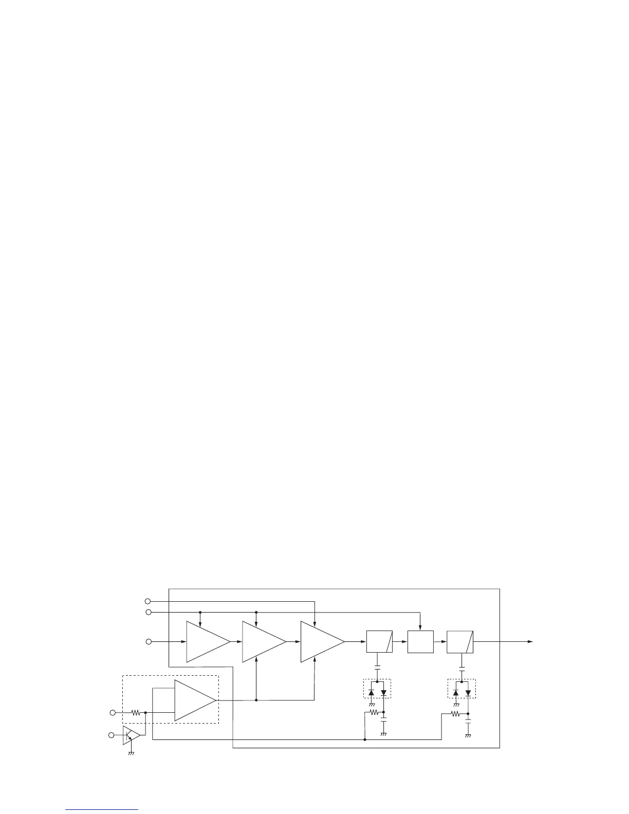
4-2-4 APC CIRCUIT (PA AND MAIN UNITS)
The APC circuit protects the drive and power amplifiers from
a mismatched output load and selects output power of HIGH
or LOW.
The power detector circuit (PA unit; D702, D703) detects the
transmit power output level and converts it into DC voltage.
The output voltage is at a minimum level when the antenna
impedance is matched with 50 Ω and is increased when it is
mismatched.
The detected voltage is applied to the differential amplifier
(MAIN unit; IC2; pin 3), and the “T2” signal from the D/A con-
verter (MAIN unit; IC12, pin 23), controlled by the CPU (MAIN
unit; IC22), is applied to the other input for reference. When
antenna impedance is mismatched, the detected voltage
exceeds the power setting voltage. Then the output voltage
of the differential amplifier (MAIN unit; IC2, pin 4) controls
the input bias voltage of the drive (PA unit; Q702) and power
(PA unit; Q701) amplifiers to reduce the output power.
• APC CIRCUIT
Power
amp.
APC
amp.
Driver
amp.
+
–
YGR
amp.
VCC
to ANT unit
PA unit
T2
TMUT
RF signal
from PLL circuit
T5V
APC control circuit
D703
D702
ANT
SW
LPF
LPF
Q702
Q704
IC2
IC501
Q701
D701
 Loading...