(No.YF123)2-27 2-28(No.YF123)
ADP_L
C101
D102
GND
3
4
2
5
1
GND
GND
TPB-
TPA+
TPB+
TPA-
5
1
2
3
4
6
BATT_+
ADP_DC
TO PARAGON
J101
QNA0040-001
DC JACK
J102
QNZ0822-001
DV JACK
MAIN(JACK)
10
yf123_y40159001a_rev0.1
TO REG
TO MAIN IF
(CN101),REG
TO CPU
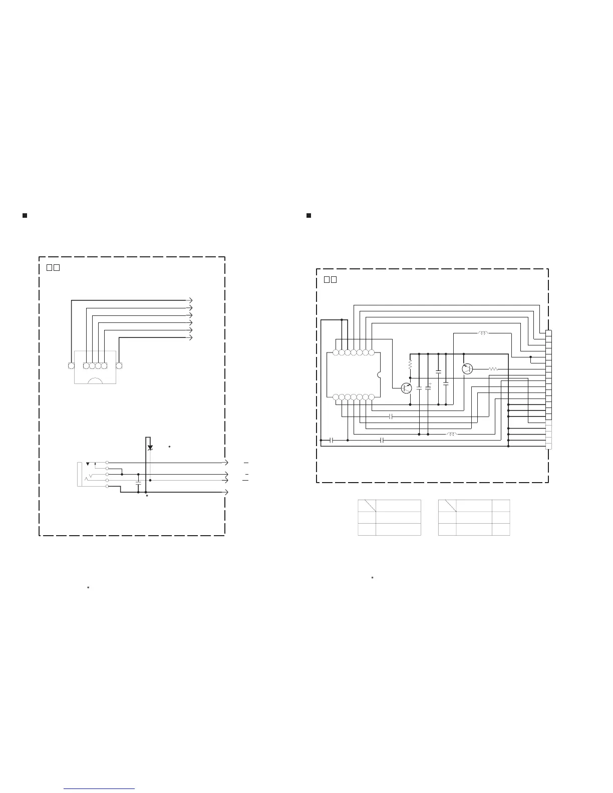
MAIN(JACK) SCHEMATIC DIAGRAM
NOTES: 1. For the destination of each signal and further line connections that are cut off from this diagram, refer to "BOARD INTERCONNECTIONS".
2. The parts with marked () is not used.
CN5001
CCD
20
yf123_y40161001a_rev1.1
Key
Ref
Dest
Key
Ref
Dest
IC5001
#
14
TEST
13
H2
12
H1
11
VL
10
SUB
9
RG
8
VDD
7
VOUT
6
GND
5
GND
4
V1
3
V2
2
V3
1
V4
Q5001
2SC3931/CD/-X
R5001
4.7k
C5004
0.1
C5002
0.1
C5007
2200p
T
C5003
OPEN
L5001
L5002
NTSC
PAL
with_DSC
w/o_DSC
4.7k
OPEN
BA8447BW-X
2SC4081/QR/-X
M6D1S3=ICX440UKM-K
M6D1S5=ICX610UKM-K
ICX611UKM-K
IC5001
OPEN
Q5002 R5002
Q5002
#
R5002
#
C5005 0.1
C5006 0.1
1V1
2V2
3V3
4V4
5 REG_15V
6 REG_15V
7 CCD_CTL
8RG
9 SUB
10 H2
11 H1
12 CCD_-7.5V
13 GND
14 GND
15 GND
16 CCD_OUT
17 GND
18 GND
19 GND
20 GND
C5001
4.7/16
10µ
10µ
TO MAIN IF
(CN4201)
CCD SCHEMATIC DIAGRAM
NOTES :1. For the destination of each signal and further line connectionsthat are cut off from this diagram, refer to "BOARD INTERCONNECTIONS".
2. The parts with marked () is not used.
3. IC5001 is incorporated in the CCD base assembly .
When IC5001 needs replacement, replace the CCD base assembly in whole because it cannot be replaced alone.
 Loading...