Do you have a question about the JVC SP-DW103 and is the answer not in the manual?
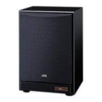
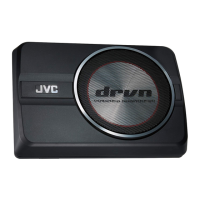
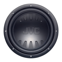
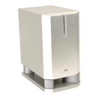
| Type | Active Subwoofer |
|---|---|
| Enclosure Type | Bass Reflex |
| Input Type | Line Level |
| Power Output | 100W |
| Driver Size | 10 inches |
Covers general safety, warnings, cautions, and critical component identification.
States that specific service instructions are not provided in this manual.
Step-by-step guide for disassembling the unit's components.
States that adjustment procedures are not provided in this manual.
States that troubleshooting procedures are not provided in this manual.
Pin layout and block diagram for the AN79L05-T regulator.
Pin layout and block diagram for the BA15218F-XE dual op-amp.
Pin layout and block diagram for the BU4584BF-X hex schmitt inverter.
Pin layout and block diagram for the IR2113S-X gate driver.
Pin layout for the NJM311M-XE comparator.
Pin layout and block diagram for the NJM78L05A-T regulator.
Pin layout and block diagram for the STR-F6676 switching regulator.
Pin layout and block diagram for the TC74HC00AF-W NAND gate IC.
Pin layout and block diagram for the TC74HC14AF-X hex schmitt inverter.
Visual representation of the system's functional blocks.
Detailed electrical circuit schematics for the unit.
Visual layouts of the internal printed circuit boards.
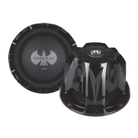
Illustrated breakdown of the amplifier section with component details.
Illustrated breakdown of the speaker section with component details.
Comprehensive list of electrical components with part numbers and descriptions.
List of packaging components and included accessories.