Hardware Principle 4-3
4.2.3 Main board
The main board could be divided into two parts: front-end of the main board and
back-end of the main board.
4.2.3.1 Front-end of the main board
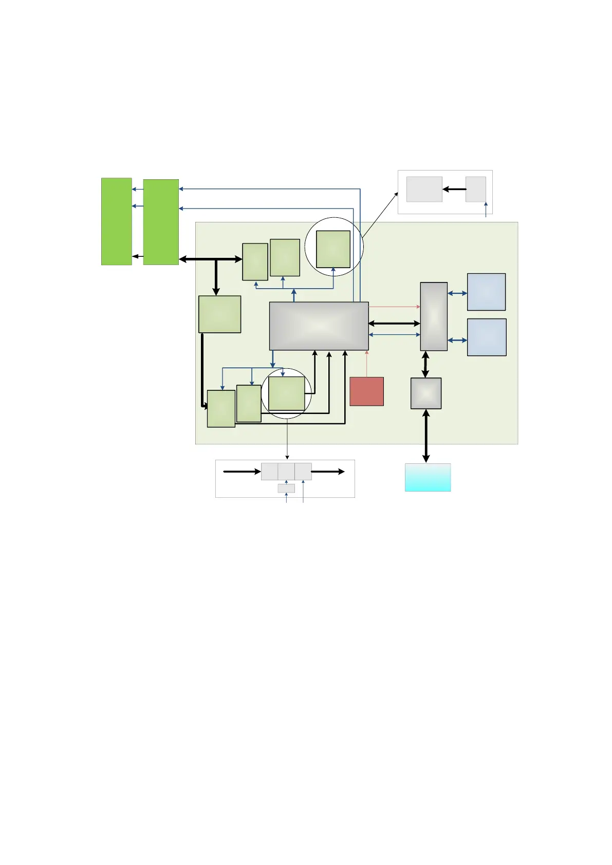
Main board
HVISO
32ch
BF FPGA
Control signal
DATA
DSP
FPGA
High-voltage control signal
IQ
DDR2
UPLOAD
DDR2
PCIE X1
CPLD control signal
Rx9~
16
Rx25~32
Rx1~8
…
...
LVDS*8
Tx9~16
Tx25~32
Tx1~8
Probe
board
PCIE
PHY
Communication
control bus
Control
signal
…
...
High-voltage
pulse output
circuit
Drive
circuit
Tx
TGC
8-channel digital
LNA VGA ADC
Rx
8-channel analog
Control signal
Control signal
CPU Module
Clock
circuit
Clock
Clock
Probe
connect
ing
board
Figure 4-3 Principle Diagram of Front-end of the Main Board
As shown in the figure above, ultrasound front-end internal structure consists of
ultrasound reception module(Rx1~Rx32), ultrasound transmission module(Tx1~Tx32),
high-voltage isolation module(HVISO), BF FPGA module, DSP FPGA
module ,PCIE_PHY module and so on.
Function describes as following:
Support 32 channel high-voltage isolation(HVISO)to protect ultrasound
reception module(Rx)to avoid ultrasound transmission high-voltage
contamination;
32 channel transmission wave forms according to scanning time sequence and
control parameters.
32 channel transmission wave forms to 32 channel high-voltage transmission
wave by driver.
Echo receiving LNA is to enlarge fixed gain.
By the control of TGC, echo receiving carries out variable gain amplification by
depth.
32 channel analog echo could be switched to 32 channel digital signal by ADC.
 Loading...