iii
Table of Contents
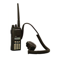
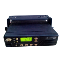
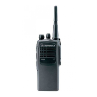
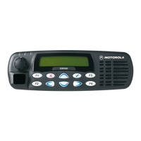
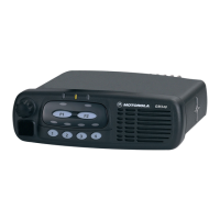
Chapter 1 MODEL CHART AND TECHNICAL SPECIFICATIONS
1.0 GP240/GP280/GP540/GP580 Model Chart.........................................................1-1
2.0 Technical Specifications ......................................................................................1-2
Chapter 2 THEORY OF OPERATION
1.0 Introduction ..........................................................................................................2-1
2.0 800 MHz Transmitter ...........................................................................................2-1
2.1 Power Amplifier ..............................................................................................2-1
2.2 Antenna Switch...............................................................................................2-2
2.3 Harmonic Filter ...............................................................................................2-2
2.4 Antenna Matching Network ............................................................................2-2
2.5 Power Control Integrated Circuit (PCIC) ........................................................2-2
3.0 800 MHz Receiver ...............................................................................................2-3
3.1 Receiver Front-End ........................................................................................2-3
3.2 Receiver Back-End.........................................................................................2-4
3.3 Automatic Gain Control (AGC) .......................................................................2-5
4.0 Frequency Generation Circuit ..............................................................................2-6
4.1 Synthesizer.....................................................................................................2-7
4.2 Voltage Controlled Oscillator (VCO)...............................................................2-8
4.3 Trunked Radio System...................................................................................2-9
Chapter 3 TROUBLESHOOTING CHARTS
1.0 Troubleshooting Flow Chart for Receiver (Sheet 1 of 2)......................................3-1
2.0 Troubleshooting Flow Chart for Receiver (Sheet 2 of 2)......................................3-2
3.0 Troubleshooting Flow Chart for Transmitter ........................................................3-3
4.0 Troubleshooting Flow Chart for Synthesizer........................................................3-4
5.0 Troubleshooting Flow Chart for VCO...................................................................3-5
6.0 Troubleshooting Flow Chart for PassPort Trunking .............................................3-6
Chapter 4 800 MHz PCB/SCHEMATICS/PARTS LISTS
1.0 Allocation of Schematics and Circuit Boards .......................................................4-1
1.1 Controller Circuits ...........................................................................................4-1
2.0 800MHz PCB 8480641Z03 / Schematics ............................................................4-3
3.0 800MHz PCB 8480641Z03 / Parts List .............................................................4-11
 Loading...