1-4 THEORY OF OPERATION
A MOSFET Q416 switches in the LiO supply when Vdd is removed. Q416 also provides isolation
from BOOT_CTRL function in the event of radio program flashing. The 3.3V regulator charges the
Lithium battery.
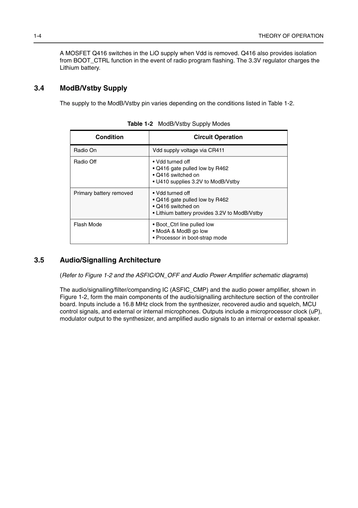
3.4 ModB/Vstby Supply
The supply to the ModB/Vstby pin varies depending on the conditions listed in Table 1-2.
3.5 Audio/Signalling Architecture
(
Refer to Figure 1-2 and the ASFIC/ON_OFF and Audio Power Amplifier schematic diagrams
)
The audio/signalling/filter/companding IC (ASFIC_CMP) and the audio power amplifier, shown in
Figure 1-2, form the main components of the audio/signalling architecture section of the controller
board. Inputs include a 16.8 MHz clock from the synthesizer, recovered audio and squelch, MCU
control signals, and external or internal microphones. Outputs include a microprocessor clock (uP),
modulator output to the synthesizer, and amplified audio signals to an internal or external speaker.
Table 1-2 ModB/Vstby Supply Modes
Condition Circuit Operation
Radio On Vdd supply voltage via CR411
Radio Off • Vdd turned off
• Q416 gate pulled low by R462
• Q416 switched on
• U410 supplies 3.2V to ModB/Vstby
Primary battery removed • Vdd turned off
• Q416 gate pulled low by R462
• Q416 switched on
• Lithium battery provides 3.2V to ModB/Vstby
Flash Mode • Boot_Ctrl line pulled low
• ModA & ModB go low
• Processor in boot-strap mode
All manuals and user guides at all-guidesbox.com
 Loading...