Circuit Descriptions, Abbreviation List, and IC Data Sheets
EN 122 Q529.1A LA9.
9. Circuit Descriptions, Abbreviation List, and IC Data Sheets
Index of this chapter:
9.1 Introduction
9.2 Main Supply
9.3 On-board DC/DC Converters
9.4 Front-End
9.5 PNX85xx
9.6 Back-end
9.7 Abbreviation List
9.8 IC Data Sheets
Notes:
•Only new circuits (circuits that are not published recently)
are described.
• Figures can deviate slightly from the actual situation, due
to different set executions.
• For a good understanding of the following circuit
descriptions, please use the wiring, block (chapter 6) and
circuit diagrams (chapter 7). Where necessary, you will find
a separate drawing for clarification.
9.1 Introduction
This chassis (member of the “TV522/92” platform) is a
derivative from the Q528.1A LA chassis (member of the
“TV520” platform). It comes with a new styling called “VE8”. In
some sets, a light strip is incorporated on the front side of the
set referred to as “Light Guide”. This generates a diffuse light
through a light pipe.
The chassis is built around the PNX85xx “System on Chip”
(SoC), which handles the video and audio processing, while
the PNX51xx takes care of the video back-end processing.
9.1.1 Features
The main features for this chassis are:
• 1080p resolution @ 100 Hz (in some sets).
• High performance back-end processing Perfect Pixel HD
engine capable of 300 Mpixels/sec. With this technology,
each pixel of the incoming picture is enhanced to better
match the surrounding pixels, resulting in a more natural
picture. Artifacts and noise in all sources from multimedia
to standard TV to highly-compressed high-definition (HD)
are detected and reduced. This results in a clean and razor
sharp image.
• ClearLCD, a technology that uses scanning and back light
dimming technology to reduce the motion blur on an LCD
screen, caused by the slow response time and the “sample
and hold” characteristic of LCD.
• The introduction of a module referred to as “Light Guide” on
the front side of the set (in some sets).
• Improved tuner compared to Q528.1A LA chassis
• For all other features: refer to the Q528.1A LA/LB Service
Manual.
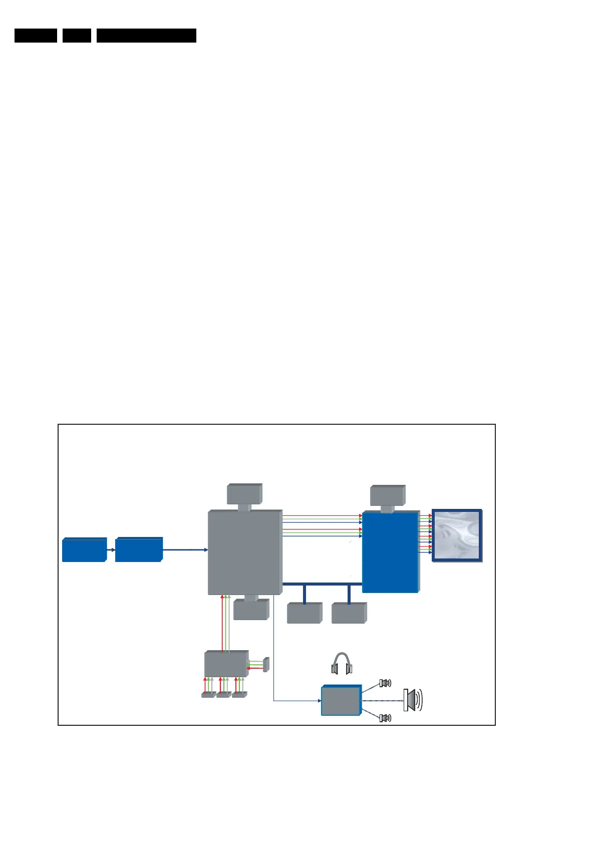
9.1.2 TV522/92 Architecture Overview
For details about the chassis block diagrams refer to chapter
“Block diagrams, Test Point Overview, and Waveforms”. An
overview of the TV522/92 architecture can be found in next
figure “Architecture of TV522/92 platform”.
Figure 9-1 Architecture of TV522/92 platform (AP region)
FLASH
8
Matrix
FHD@120p
FHD@100p
Matrix
FHD@120p
FHD@100p
PNX5100
Halo Free
HD-NM
FHD 100Hz
PCI
2 channel
Audio Amp.
32
DDR-II
TV522/92 Architecture Block Diagram (AP region)
Hybrid Tuner
Saw
MASTER IF
Ethernet
NXP
PNX8541
USB2.0
32
DDR-II
HDMI
MUX
hdmi hdmi hdmi
hdmi
I_17670_005.eps
280408
 Loading...