GSM/GPRS/NB-IoT Module Series
BC68&M66 Compatible Design
BC68&M66_Compatible_Design 21 / 31
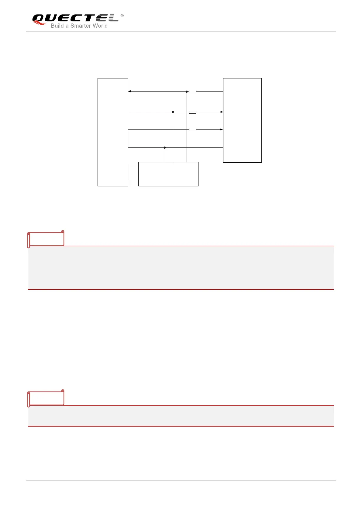
If the DTE is 3.0V or 3.3V power domain, a reference design of 3.3V level match for BC68 is shown as
below.
DTE
TXD
RXD
1K
TXD
RXD
RI
RI
BC68
Voltage level: 3.3V
1K
1K
GND
GND
TXD
RXD
GND
TEST POINTS
RESET
VBAT
VBAT
RESET
Figure 13: Reference Design of BC68 UART Interface for 3.3V System
1. In order to reduce the power consumption of the system, it is highly recommended to add resistors
with resistance greater than 1KΩ on the UART port signal traces when the host’s voltage level is 3.0V
or 3.3V.
2. It is recommended to reserve the test points (RXD, TXD, RESET and VBAT) for firmware upgrading.
4.8. ADC Interface
The pin ADC* of BC68 module and the pin ADC0 of M66 provide a 10-bit ADC input channel to read the
voltage value. In addition, M66 offers an AVDD pin to provide a reference voltage for ADC0 and the max
voltage of AVDD is 2.8V. In order to improve the accuracy of ADC, the layout of ADC should be
surrounded by ground.
“*” means under development.

 Loading...