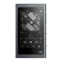
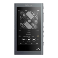
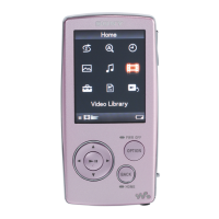
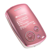
NW-A1000
2323
NW-A1000
Note on Schematic Diagram:
• All capacitors are in µF unless otherwise noted. (p: pF)
50 WV or less are not indicated except for electrolytics
and tantalums.
• All resistors are in Ω and
1
/
4
W or less unless otherwise
specified.
• f : internal component.
• C : panel designation.
• A : B+ Line.
• Power voltage is dc 4.2 V and fed with regulated dc power
supply from TP9001 and TP9002 on the MAIN board.
• Voltages and waveforms are dc with respect to ground
under no-signal conditions.
no mark : PLAYBACK
• Voltages are taken with a VOM (Input impedance 10 MΩ).
Voltage variations may be noted due to normal produc-
tion tolerances.
• Waveforms are taken with a oscilloscope.
Voltage variations may be noted due to normal produc-
tion tolerances.
• Circled numbers refer to waveforms.
• Signal path.
F : AUDIO
Note on Printed Wiring Board:
• X : parts extracted from the component side.
• Y : parts extracted from the conductor side.
• f : internal component.
• : Pattern from the side which enables seeing.
(The other layers' patterns are not indicated.)
Caution:
Pattern face side: Parts on the pattern face side seen from
(Conductor Side) the pattern face are indicated.
Parts face side: Parts on the parts face side seen from
(Component Side) the parts face are indicated.
surfac
• The voltage and waveform of CSP (chip size package)
cannot be measured, because its lead layout is different
from that of conventional IC.
• Waveforms
• MAIN board is multi-layer printed board.
However, the patterns of intermediate-layer have not been
included in diagram.
• Lead Layouts
* Replacement of IC3101, 5001, 6005, 7001, 8001 and
9001 used in this set requires a special tool.
• Note for Printed Wiring Boards and Schematic Diagrams
Lead layout of conventional IC CSP (chip size package)
* Replacement of IC3101, 5001, 6005, 7001, 8001 and
9001 used in this set requires a special tool.
Note:
The components identi-
fied by mark 0 or dotted
line with mark 0 are criti-
cal for safety.
Replace only with part
number specified.
Note:
Les composants identifiés par
une marque 0 sont critiques
pour la sécurité.
Ne les remplacer que par une
pièce portant le numéro
spécifié.
2
IC4101 8 (OSCOUT)
500 mV/DIV, 10
µ
s/DIV
30.5
µ
s
1.1 Vp-p
3
X3101
2 V/DIV, 20 ns/DIV
44.3 ns
3.6 Vp-p
1
X6001
1 V/DIV, 20 ns/DIV
44.3 ns
2.3 Vp-p
4
IC3002 2 (BCK)
2 V/DIV, 100 ns/DIV
326 ns
3.4 Vp-p
5
IC3002 qh (SCKI)
2 V/DIV, 50 ns/DIV
89 ns
4.3 Vp-p
22.8
µ
s
3.5 Vp-p
6
IC3002 w; (LRCK)
2 V/DIV, 10
µ
s/DIV
7
X5001
1 V/DIV, 50 ns/DIV
89 ns
2.8 Vp-p
 Loading...