DocID028599 Rev 7 29/82
UM1974 Hardware layout and configuration
81
6.12 Solder bridges
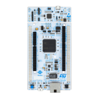
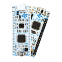
SBxx can be found on top layer and SB1xx can be found on bottom layer of the Nucleo-144
board.
PG13 RXII TXD0 - SB182 ON SB182 OFF
PB13 RMII TXD1 I2S_A_CK JP7 ON JP7 OFF
Table 11. Ethernet pins (continued)
Pin
name
Function
Conflict with
ST Zio connector
signal
Configuration when using
Ethernet
Configuration when using
ST Zio or ST morpho
connector
Table 12. Solder bridges
Bridge State
(1)
Description
SB2 (+3.3 V_PER)
ON Peripheral power +3.3V_PER is connected to +3.3 V.
OFF Peripheral power +3.3V_PER is not connected.
SB3 (3.3 V)
ON Output of voltage regulator LD39050PU33R is connected to 3.3 V.
OFF Output of voltage regulator LD39050PU33R is not connected.
SB7, SB4 (GPIO)
ON
PD8 and PD9 on STM32 are connected to ST morpho connectors CN11
and CN12. If these pins are used on ST morpho connectors, SB5 and
SB6 should be OFF.
OFF
PD8 and PD9 on STM32 are disconnected to ST morpho connectors
CN11 and CN12.
SB5, SB6 (ST-LINK-USART)
ON
PA2 and PA3 on ST-LINK STM32F103CBT6 are connected to PD8 and
PD9 to enable virtual COM port for mbed support. Thus PD8 and PD9 on
ST morpho connectors cannot be used.
OFF
PA2 and PA3 on ST-LINK STM32F103CBT6 are disconnected to PD8
and PD9 on STM32.
SB12 (V
DDA
)
ON V
DDA
and V
REF+
on STM32 is connected to V
DD
.
OFF
V
DDA
and V
REF+
on STM32 is not connected to V
DD
and can be provided
from pin 6 of CN7 (Used for external V
REF+
provided by Arduino shield).
SB101,103,105,108
(DEFAULT)
ON Reserved, do not modify.
SB102,104,106,109
(RESERVED)
OFF Reserved, do not modify.
SB107 (STM_RST)
OFF No incidence on ST-LINK STM32F103CBT6 NRST signal.
ON
ST-LINK STM32F103CBT6 NRST signal is connected to GND
(ST-LINK reset to reduce power consumption).
SB110 (SWO)
ON SWO signal of the STM32 (PB3) is connected to ST-LINK SWO input.
OFF SWO signal of STM32 is not connected.
 Loading...