B2.10
T855 Circuit Operation
M850-00
31/09/98 Copyright TEL
2.10 Synthesised Local Oscillator
(Refer to the synthesiser circuit diagram (sheet 7) in Section 6.3 and the VCO circuit dia-
gram in Part E.)
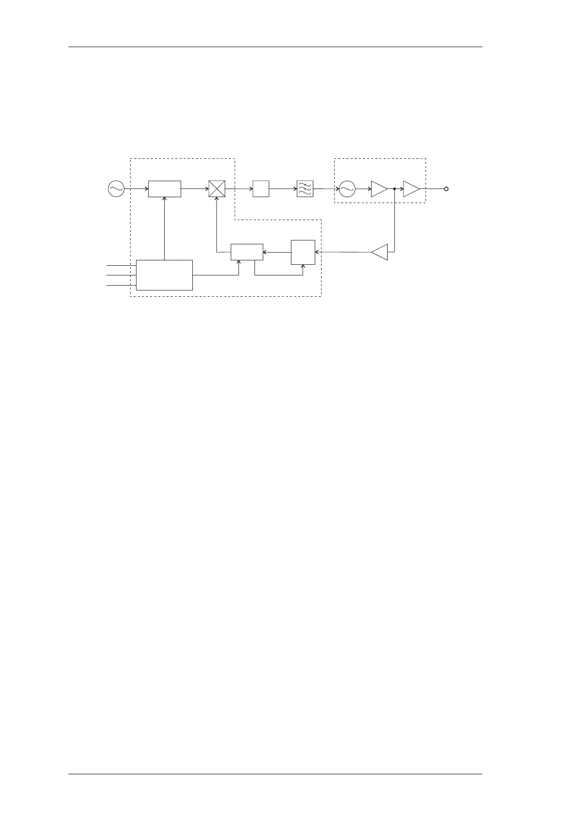
Figure 2.6 T855 Synthesiser Block Diagram
The synthesiser (IC740) employs a phase-locked loop (PLL) to lock a voltage controlled
oscillator (VCO) to a given reference frequency. The synthesiser receives the divider
information from the control microprocessor via a 3-wire serial bus (clock, data, enable).
When the data has been latched in, the synthesiser processes the incoming signals from
the VCO buffer (f
in
) and the reference oscillator (f
ref
).
A reference oscillator at 12.8MHz (IC700) is buffered (IC710) and divided down to
6.25kHz or 5kHz within the synthesiser IC (IC740).
A buffered output of the VCO is divided with a prescaler and programmable divider
which is incorporated into the synthesiser chip (IC740). This signal is compared with
the reference signal at the phase detector (also part of the synthesiser chip). The phase
detector outputs drive a balanced charge pump circuit (Q760, Q770, Q775, Q780, Q785)
and active loop filter (IC750, Q790) which produces a DC voltage between 0V and 20V
to tune the VCO. This VCO control line is further filtered to attenuate noise and other
spurious signals. Note that the VCO frequency increases with increasing control volt-
age.
12.8MHz
Reference
Oscillator
Serial
Bus
/R
Reference
Divider
Phase
Detector
Charge
Pump
Loop
Filter
VCO PCB
FREQUENCY SYNTHESISER IC
VCO Buffer
Output
Buffer
+22dBm
L.O.
Clk
Data
En
Controller
Buffer
f
in
f
ref
/N
Programmable
Divider
64/65
Prescaler