2465B/2467B Service
LIST OF ILLUSTRATIONS
Figure Page
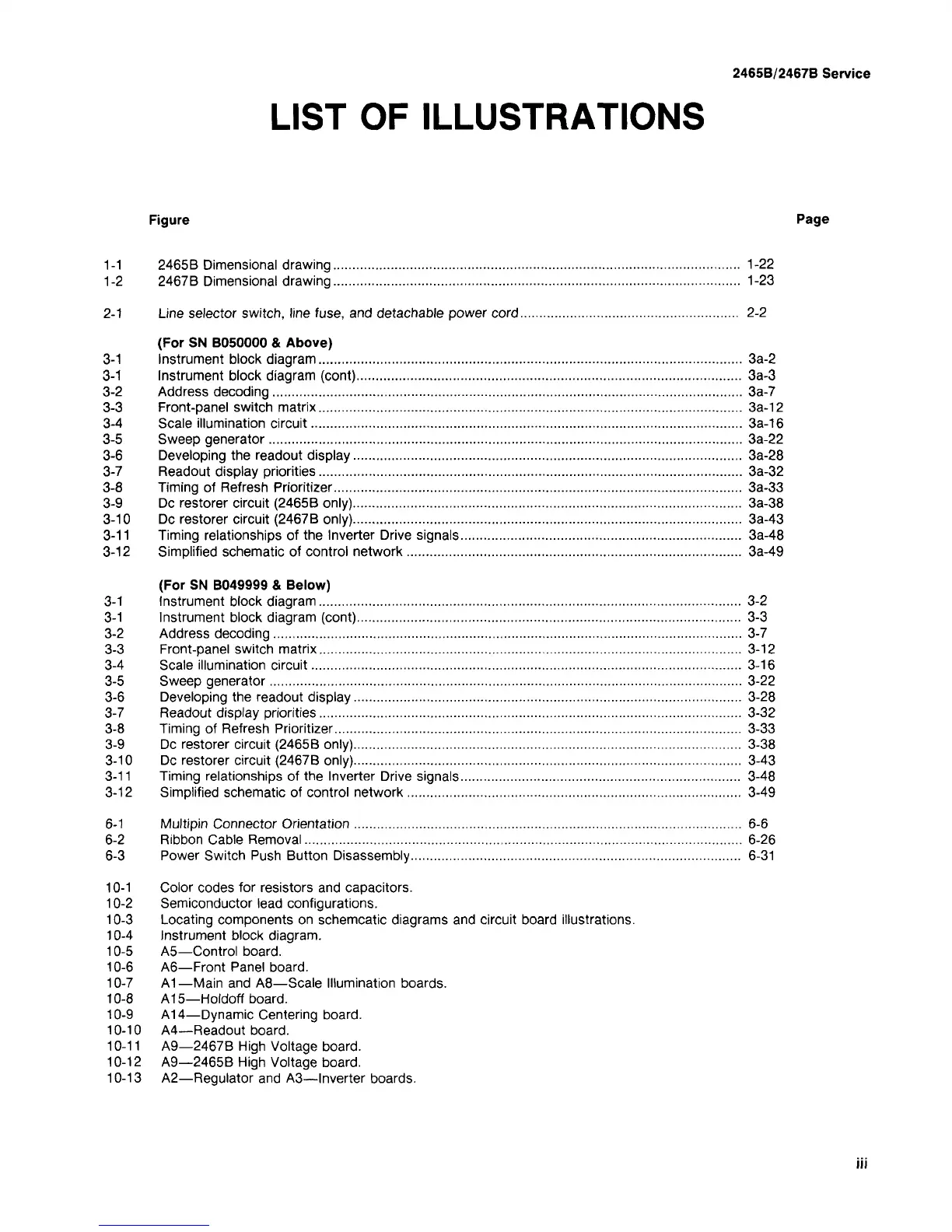
1-1 2465B Dimensional drawing 1-22
1-2 2467B Dimensional drawing 1-23
2-1 Line selector switch, line fuse, and detachable power cord 2-2
(For SN B050000 & Above)
3-1 Instrument block diagram 3a-2
3-1 Instrument block diagram (cont) 3a-3
3-2 Address decoding 3a-7
3-3 Front-panel switch matrix 3a-12
3-4 Scale illumination circuit 3a-16
3-5 Sweep generator 3a-22
3-6 Developing the readout display 3a-28
3-7 Readout display priorities 3a-32
3-8 Timing of Refresh Prioritizer 3a-33
3-9 Dc restorer circuit (2465B only) 3a-38
3-10 Dc restorer circuit (2467B only) 3a-43
3-11 Timing relationships of the Inverter Drive signals 3a-48
3-12 Simplified schematic of control network 3a-49
(For SN B049999 & Below)
3-1 Instrument block diagram 3-2
3-1 Instrument block diagram (cont) 3-3
3-2 Address decoding 3-7
3-3 Front-panel switch matrix 3-12
3-4 Scale illumination circuit 3-16
3-5 Sweep generator 3-22
3-6 Developing the readout display 3-28
3-7 Readout display priorities 3-32
3-8 Timing of Refresh Prioritizer 3-33
3-9 Dc restorer circuit (2465B only) 3-38
3-10 Dc restorer circuit (2467B only) 3-43
3-11 Timing relationships of the Inverter Drive signals 3-48
3-12 Simplified schematic of control network 3-49
6-1 Multipin Connector Orientation 6-6
6-2 Ribbon Cable Removal 6-26
6-3 Power Switch Push Button Disassembly 6-31
10-1 Color codes for resistors and capacitors.
10-2 Semiconductor lead configurations.
10-3 Locating components on schemcatic diagrams and circuit board illustrations.
10-4 Instrument block diagram.
10-5 A5—Control board.
10-6 A6—Front Panel board.
10-7 A1—Main and A8—Scale Illumination boards.
10-8 A15—Holdoff board.
10-9 A14—Dynamic Centering board.
10-10 A4—Readout board.
10-11 A9—2467B High Voltage board.
10-12 A9—2465B High Voltage board.
10-13 A2—Regulator and A3—Inverter boards.
in

 Loading...