VCXO Phase Noise 122.88 MHz
www.ti.com
30
SNAU145B–MAY 2013–Revised March 2018
Submit Documentation Feedback
Copyright © 2013–2018, Texas Instruments Incorporated
Typical Phase Noise Performance Plots
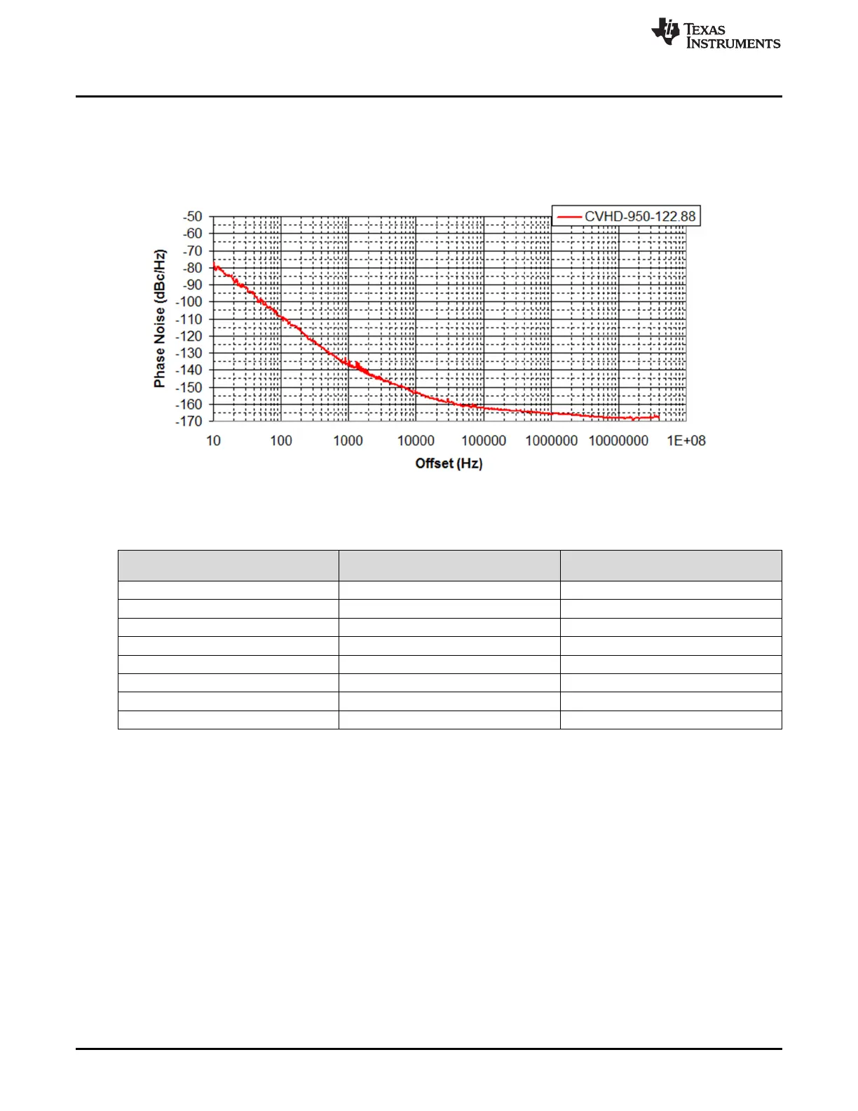
B.1 VCXO Phase Noise 122.88 MHz
The phase noise of the reference is masked by the phase noise of this VCXO by using a narrow loop
bandwidth for PLL1 while retaining the frequency accuracy of the reference clock input. This VCXO sets
the reference noise to PLL2. Figure 19 shows the open loop typical phase noise performance of the
CVHD-950-122.88 Crystek VCXO.
Figure 19. Crystek CVHD-950-122.88 MHz VCXO Phase Noise at 122.88 MHz
Table 7. VCXO Phase Noise and Jitter
Offset
VCXO Phase Noise
at 122.88 MHz (dBc/Hz)
VCXO RMS Jitter to High Offset
of 20 MHz at 122.88 MHz (rms fs)
10 Hz -76.6 515.4
100 Hz -108.9 60.5
1 kHz -137.4 36.2
10 kHz -153.3 35
100 kHz -162 34.5
1 MHz -165.7 32.9
10 MHz -168.1 22.7
40 MHz -168.1 —
B.2 Output Measurement Technique
The same technique was used to measure phase noise for all three output types available on the
programmable OSCout and CLKout buffers. This was achieved by terminating one side of the LVPECL,
LVDS, or LVCMOS output with a 50-Ω load, and measuring the other side single-ended using an Agilent
E5052B Source Signal Analyzer.
B.3 Clock Outputs (DCLKout and SDCLKout)
The LMK0482x features programmable HSDS, LVDS, LVPECL buffer modes for the DCLKoutX,
SDCLKout pairs. Below is a phase noise measurement of DCLKout2 (best phase noise clock output)
using both a balun and single ended.
 Loading...