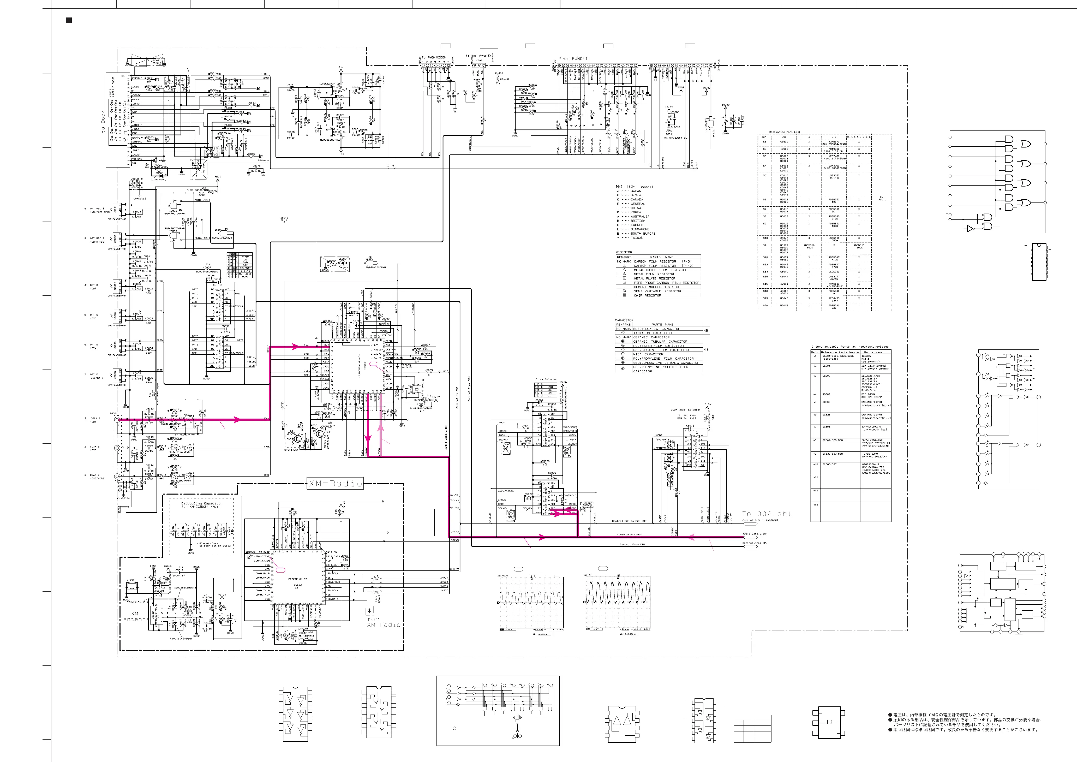
CB501
CB502
IC501 IC501
IC501 IC501
IC501 IC501
IC505 IC504
IC502
IC502
IC502
IC510
IC510
IC502
IC503
IC506
IC511
IC512
CB505
CB503
W5001
CB504
IC508
IC509
IC507
A
1
2
3
4
5
6
7
8
9
10
BCDEFGH I JK
L MN
RX-V3800/DSP-AX3800
123
★ All voltages are measured with a 10MΩ/V DC electronic voltmeter.
★ Components having special characteristics are marked s and must be replaced
with parts having specifications equal to those originally installed.
★ Schematic diagram is subject to change without notice.
DSP 1/3
SCHEMATIC DIAGRAMS
B-1
POINT B-1 XL502 (Pin 29 of IC506)
5.0
5.0
5.0
5.0
1
2
4
9
11
12
13
10
5
3
6
8
5.0
3.3
3.3
0
0
0
0
0
5.0
5.0
0
0
4.1
0
0
4.1 4.8
4.1 4.1
0
4.1
5.0 0
3.9
3.3
3.3
0
3.3
3.3
0
0
0
4.1
4.8
4.1
4.1
4.1
0
5.0
0
3.9
0
0
4.1
4.1
0
4.8
4.8
0
2.3
2.3
2.3 2.7
3.0
0
0
0
0.1
0
0
3.2
3.3
3.3
0
0
3.3
3.3
0
0
0
0
0
1.6
1.6
0
1.6
1.6
0
3.2
0
0
1.6
3.3
0
3.3
3.3
0.2
0
3.3
0
3.3
3.3
0
0
0
00
0
0
0
1.6
0
0
1.6
0
0
1.2
0
1.6
1.6
0
0.5
0
0
3.3
0
3.3
3.3
4.8
3.2
0
0
0.2
0.2
3.3
0
1.6
1.6
0
3.3
1.6
0
1.3
0.2
0.2
0.2
0.2
12.4
0.2
0.2
-11.9
1.6
3.3
0
1.6
3.3
0
1.3
3.3
0
1.6
3.3
0
0
3.3
0
3.3
3.2
4.8 4.8
0
0.6
0.5
0
3.3
3.9
3.9
0
3.3
0
3.3
3.3
0
0
0
0
3.3
1.6
1.6
3.3
0
0.5
0
0
3.2
1.2
0
3.2
3.2
0
1.6
3.3
1.6
0
2.0
0
0
3.3
0
1.2
3.2
3.2
0
0
0
0
0
3.2
3.2
3.2
1.5
3.3
0
1.2
0
3.2
0
0
0
3.3
3.2
0
0
2.7 0.6
2.7
0.5
0
4.8
4.8
4.8
4.1
D-2
POINT D-2 Pin 14 of IC503
ANALOG IN
ANALOG IN
DIGITAL IN
DIGITAL IN
Input
Selector
RXOUT
RX0
RX1
RX2
RX3
RX4
RX5/VI
RX6/UI
LPF
TMCK/PIO0
TBCK/PIO1
TLRCK/PIO2
TDATA/PIO3
TXO/PIOEN
Cbit, Ubit
Microcontroller
I/F
Data
Selector
Clock
Selector
Modulation
&
Parallel Port
PLL
XIN XOUT XMCK CKST
SLRCK
SBCK
RLRCK
RBCK
RMCK
SDIN
RDATA
RERR
DO
XMODECICECLINTAUDIO/VOEMPHA/UO
1/N
Demodulation
&
Lock detect
1
2
3
4
5
8
9
10
13
44
45
46
47
48
29 28 27 34
23
22
20
17
16
24
21
36
37
41383940353332
IC506: LC89057W-VF4AD-E
Digital audio interface transceiver
IC510: NJM2068MD-TE2
Dual operational amplifier
OUT1
OUT2
–IN1
+IN1
+IN2
-IN2
–VCC
+VCC
1
2
3
4
8
7
6
5
+
–
+
–
4B13
4A12
4Y11
3B10
3A9
3Y8
1B 2
1Y 3
2A 4
2B 5
2Y 6
GND 7
IC502: SN74AHCT00PWR
Quadruple 2-input NAND gate
Vcc141A 1
S
2
S
1
S
0
E
I
0
I
1
I
2
I
3
I
4
I
5
I
6
I
7
Z
Z
1412
6
7
34
5
9
11
12
10
1315
V
CC
= PIN 16
GND = PIN 8
= PIN NUMBERS
IC504, 505: SN74LS151NSR
8-input multiplexer
IC509: SN74LV157APWR
Quadruple 2-line to 1-line data selectors/multiplexers
Pin numbers shown are for the D, DB, DGV, J, NS, PW, and W packages.
2
3
5
6
11
10
14
13
15
1
G
A/B
4B
4A
3B
3A
2B
2A
1B
1A
4
7
9
12
1Y
2Y
3Y
4Y
1
2
3
4
5
6
7
8
16
15
14
13
12
11
10
9
A/B
1A
1B
1Y
2A
2B
2Y
GND
V
CC
G
4A
4B
4Y
3A
3B
3Y
IC501: SN74LVU04APWR
Hex inverters
GND
Y3
A3
A2
A1
VCC
A6
A5
A4
Y6
Y5
Y4
Y2
Y1
1
2
3
4
5
6
7
14
13
12
11
10
9
8
IC507, 508: TC74VHC153FT
Dual 4-channel multiplexer
14
A
S0
S0
6
1C0
2
B
S1
S1
S2
S2
S3
S3
S0
7
1Y
5
1C1
S1
4
1C2
S2
1
1G
3
1C3
S3
10
2C0
S0
9
2Y
11
2C1
S1
12
2C2
S2
15
2G
13
2C3
S3
1
3
2
5
4
GND
V
CC
IC512: TC7SH08FU
2-input AND gate
IN A
IN B
OUT Y
IC511: TC74VHC125FT
high speed CMOS quad bus buffer
11G
21A
31Y
42G
52A
62Y
7
14
13
12
11
10
9
8GND
Vcc
4G
4A
4Y
3G
3A
3Y
inputs outputs
GY
HZ
LL
L
A
X
L
HH
to DSP 2/3
No replacement part available.
サービス部品供給なし
DIR
INPUT
SELECT
REC OUT
SELECT
DUTY CORRECTOR
XM DT
(U, C models)
to FUNCTION (1)_CB411
Page 126
J9
to OPERATION (3)_CB805
Page 130 E2
to FL (2)_CB954
Page 141 C8
to FL (2)_CB974
Page 141 D8
XM
DOCK
 Loading...