1
1
2
2
3
3
4
4
5
5
6
6
7
7
8
8
A A
B B
C C
D D
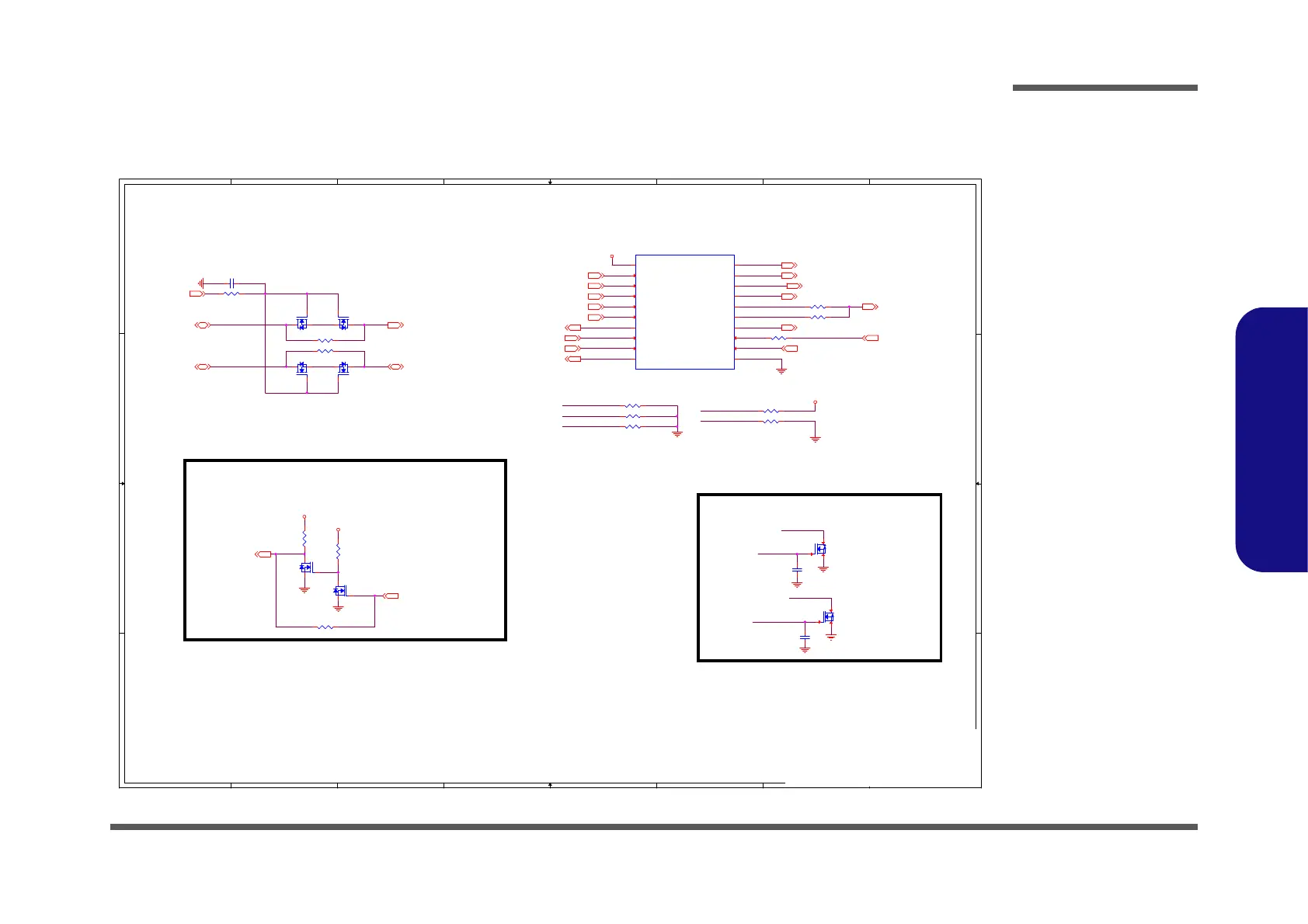
HW POWER DOWN SEQUENCE
NVIDIA GPIO LEVEL SHIFT
DEFAULT HW POWER SEQUENCE
EC SM_BUS
GPU SM_BUS
From EC
Try to cost down
Try to cost down
3.3VS
3.3VS
3.3VA
1V8_AON
DGPU_PWRGD 66
DGPU_PWRGD_R4
NV_PEXVDD_EN 27,65
NV_FBVDDQ_EN 66
DGPU_PWR_EN 4,51
NV_1V8AON_EN 67
NV_EN_DOWN39
GPIO1_GC6_FB_EN30,34,67
OVERT#30
1V8_AON_PWRGD67
PLT_RST#9,39
DGPU_RST#_PCH11,30
NV_NVVDD_EN 63,64
EC_GPIO51,57,63,66
SMC_BAT51,57,62,72
SMD_BAT51,57,62,72
NVVDD_PWRGD15,63
I2CC_SDA_PP 30,63,66
I2CC_SCL_PP 30,63,66
GPIO4_GC6_NVVDD_EN 7,30
GC6_FB_EN_PCH7,51
GPU_PEX_RST#15,30
NV_NV3V3_EN 67
OVERT#_EC 51
Title
Size Document Number Rev
Date: Sheet
of
6-71-NP5P0-D02
D02
[33] NVIDIA POWER SEQUENCE
A3
33 72Wednesday, December 29, 2021
ᙔ!Ϻ!ႝ!တ!!DMFWP!DP/
ADL-H+GN20-E3
Title
Size Document Number Rev
Date: Sheet
of
6-71-NP5P0-D02
D02
[33] NVIDIA POWER SEQUENCE
A3
33 72Wednesday, December 29, 2021
ᙔ!Ϻ!ႝ!တ!!DMFWP!DP/
ADL-H+GN20-E3
Title
Size Document Number Rev
Date: Sheet
of
6-71-NP5P0-D02
D02
[33] NVIDIA POWER SEQUENCE
A3
33 72Wednesday, December 29, 2021
ᙔ!Ϻ!ႝ!တ!!DMFWP!DP/
ADL-H+GN20-E3
U59
SLG4U44644VTR
VDD
1
VIN_DOW N
2
OVERT#
3
SUSB#
4
NVVDDS_PWRGD
5
GC6_FB_EN
6
GC6_FB_EN_PCH
7
PLT_RST#
8
dGPU_RST#_PCH
9
GPU_PEX_RST#
10
FBVDDQ_EN
20
PEX_VDD_EN
19
NVVDDS_EN
18
NVVDD_EN
17
3V3_SYS_EN
16
1V8_MAIN_EN
15
1V8_AON_EN
14
GPIO4_1V8_MAIN_EN
13
dGPU_PWR_EN
12
GND
11
Q58
SM3018KWH
G
DS
S
D
G
Q12B
*MTDK3S6R
5
34
R444 *200K_04
C1042
*0.1u_10V_X7R_04
Q56
SM3018KWH
G
DS
R940 0_04
R952
*100K_04
C691 *0.1u_10V_X7R_04
R951 *0_04
S
D
G
Q57B
*MTDK3S6R
5
34
R445 0_04
R950 0_04
R949 0_04
S
D
G
Q57A
*MTDK3S6R
2
61
S
D
G
Q11A
*MTDK3S6R
2
6 1
R941 *100K_04
R927 *100K_04
S
D
G
Q11B
*MTDK3S6R
5
34
R948 100K_04
S
D
G
Q12A
*MTDK3S6R
2
6 1
C1031
*0.1u_10V_X7R_04
R947
*100K_04
R926 100K_04
R441 0_04
R943 10K_04
NV_NVVDD_EN
NV_EN_DOWN
NV_EN_DOWN
NV_FBVDDQ_EN
NV_1V8RUN_EN
DGPU_PWR_EN
GC6_FB_EN_PCH
DGPU_RST#_PCH
GC6_FB_EN_PCH
DGPU_RST#_PCH
DGPU_PWR_EN
GPU_PEX_RST#
GPU_PEX_RST#
GPU_PEX_RST#
SMC_BAT
SMD_BAT
GPIO4_GC6_NVVDD_EN
 Loading...