


A
Amber ChristianAug 21, 2025
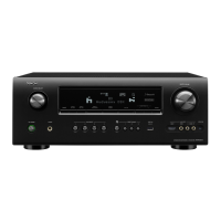
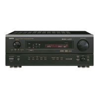
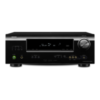
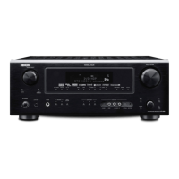
Why is there no audio output from my Denon AVR-3311CI Stereo Receiver?
- RRobert SanchezAug 21, 2025
Several factors could be at play. First, ensure all device connections and speaker connections are secure. Verify that the audio device is powered on and the master volume is appropriately adjusted. Also, check that mute mode is off and that a suitable input source and mode are selected. If headphones are connected, disconnect them, as this will prevent sound output from the speakers or PRE OUT connectors.