25
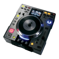
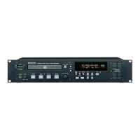
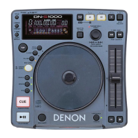
DN-S1000
64M SDRAM (IC210)
128M SDRAM (IC402)
BU2090F (IC602)
TPC6103 (IC410)
154
27 28
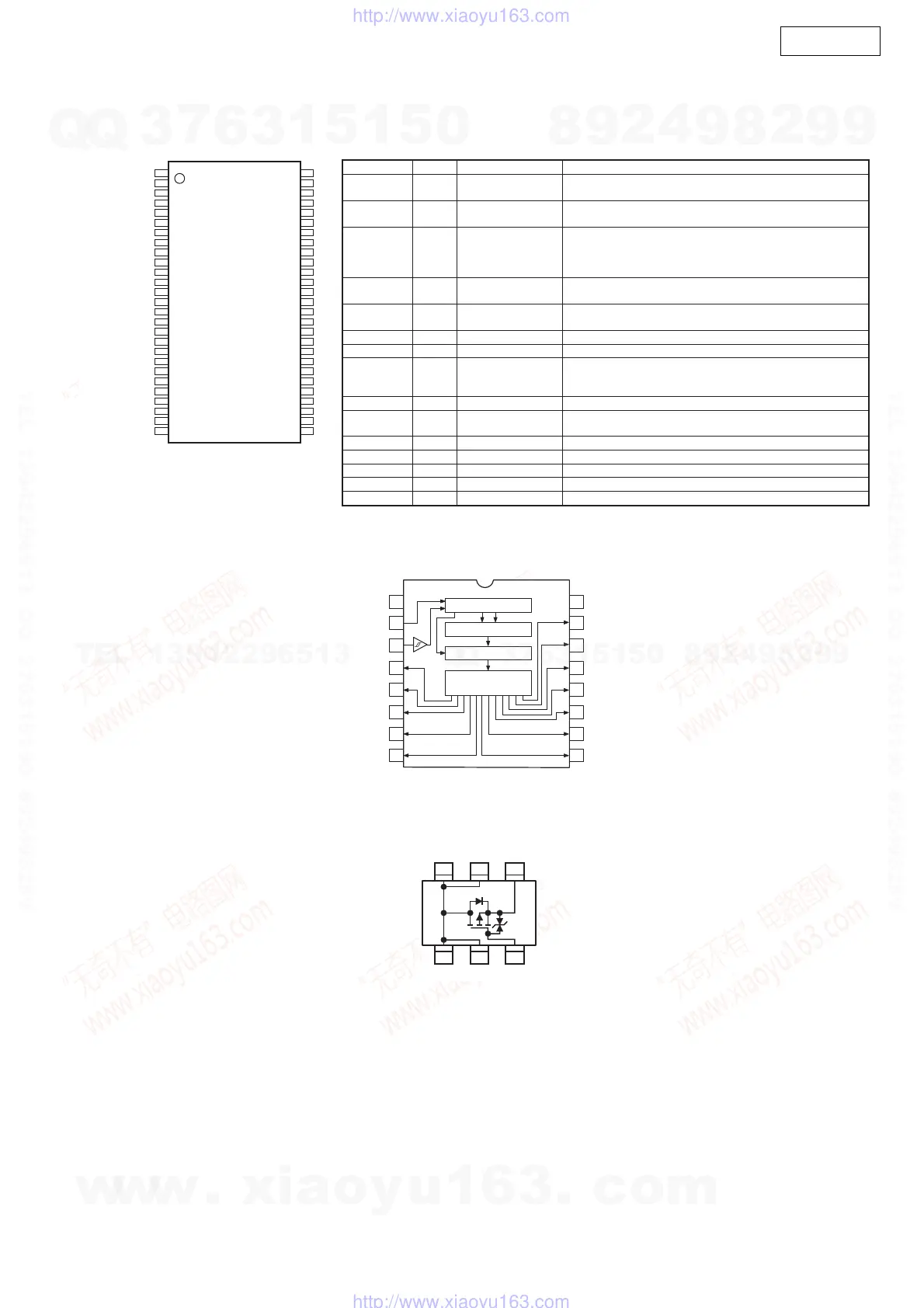
TOP VIEW
Pin Assignment
DescriptionPin No.
Pin Name
Function
22, 23~26, A0~A11 Address Multiplexed pins for row and column address.
29~35 Row address: A0~A11. Column address: A0~A8.
20, 21 BS0, Bank Select Select bank to activate during row address latch time, or bank to
BS1 read/write during address latch time.
2, 4, 5, 7, 8, DQ0~ Data Input/Output Multiplexed pins for data output and input.
10,11, 13, 42, DQ15
44,45, 47, 48,
50, 51, 53
19 CS# Chip Select Disable or enable the command decoder. When command decoder is
disabled, new command is ignored and previous operation continues.
18 RAS# Row Address Strobe Command input. When sampled at the rising edge of the clock,
RAS#, CAS# and WE# define the operation to be executed.
17 CAS#
Column Address Strobe
Referred to RAS#
16 WE# Write Enable Referred to RAS#
15, 39 UDQM/ input/output mask The output buffer is placed at Hi-A (with latency of 2) when DQM is
LDQM sampled high in read cycle. In write cycle, sampling DQM high will
block the write operation with zero latency.
38 CLK Clock Inputs System clock used to sample inputs on the rising edge of clock.
37 CKE Clock Enable CKE controls the clock activation and deactivation. When CKE is low,
Power Down mode, Suspend mode, or Self Refresh mode is entered.
1, 14, 27 Vcc Power (+3.3V) Power for input buffers and logic circuit inside DRAM.
28, 41, 54 Vss Ground Ground for input buffers and logic circuit inside DRAM.
3, 9, 43, 49 VccQ
Power (+3.3V) for I/O buffer
Separated power from Vcc, used for output buffers to improve noise.
6, 12, 46, 52 VssQ Ground for I/O buffer Separated ground from Vss, used for output buffers to improve noise.
36, 40 NC No Connection No Connection
16 VDD1Vss
15 Q112DATA
14 Q103CLOCK
13 Q94Q0
12 Q85Q1
11 Q76Q2
10 Q6
Q5
7Q3
9
8Q4
Control Circuit
12-Bit Shift Register
Latch
Output Buffer
(Open Drain)
654
123
w
w
w
.
x
i
a
o
y
u
1
6
3
.
c
o
m
Q
Q
3
7
6
3
1
5
1
5
0
9
9
2
8
9
4
2
9
8
T
E
L
1
3
9
4
2
2
9
6
5
1
3
9
9
2
8
9
4
2
9
8
0
5
1
5
1
3
6
7
3
Q
Q
TEL 13942296513 QQ 376315150 892498299
TEL 13942296513 QQ 376315150 892498299
http://www.xiaoyu163.com
http://www.xiaoyu163.com
 Loading...