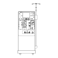
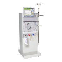
Fresenius Medical Care 4008 HDF 3/11.97 (TM) 4-1
Table of contents
4 Circuit descriptions and circuit diagrams
Section Page
Fig.: Connection diagram 4008 HDF .............................................................................. 4-3
Fig.: Wiring diagram 4008 HDF ...................................................................................... 4-5
Fig.: Block circuit diagram, mains voltage 4008 HDF .................................................... 4-7
Fig.: Block circuit diagram, low voltage 4008 HDF ........................................................ 4-7
4.1 LP 625 display board .................................................................................................... 4-9
4.1.1 Description ...................................................................................................................... 4-9
4.1.2 Circuit and component layout diagram ........................................................................... 4-11
4.2 LP 754 control board HDF............................................................................................ 4-15
4.2.1 Description ...................................................................................................................... 4-15
4.2.2 Circuit and component layout diagram ........................................................................... 4-17
4.3 LP 760 HDF motor control............................................................................................ 4-23
4.3.1 Description ...................................................................................................................... 4-23
4.3.2 Circuit and component layout diagram ........................................................................... 4-25
4.4 LP 761 HDF drive keyboard ......................................................................................... 4-29
4.4.1 Description ...................................................................................................................... 4-29
4.4.2 Circuit and component layout diagram ........................................................................... 4-31
4.5 LP 762 scales comm..................................................................................................... 4-35
4.5.1 Description ...................................................................................................................... 4-35
4.5.2 Circuit and component layout diagram ........................................................................... 4-37
4.6 LP 763 serial interface extender .................................................................................. 4-41
4.6.1 Description ...................................................................................................................... 4-41
4.6.2 Circuit and component layout diagram ........................................................................... 4-43
 Loading...