10
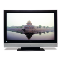
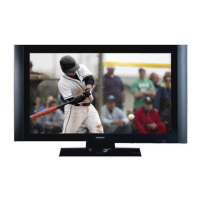
AV3000 AVC Unit Service Manual
4.6.1.
SDA5550
Micro-controller (IC704)
Supply voltage: +3.3VSTB at pin 8, 40, 75 and 92 and +2.5VSTB at pin 6, 22, 56 and 73.
Control through I
2
C: SDA3v3 at pin 52 and SCL3v3 at pin 47.
3 wire bus: 3WB-clock3v3 at pin 41 and 3WB-data3v3 at pin 46:
• FC-enable at pin 42
• MSC-enable at pin 43
• OSD enable at pin 44
Control through/by AVlink: output at pin 16 and input at pin 33.
RS232C (19200bps): TxD3v3 at pin 32 and RxD3v3 at pin 38.
Control by I/R in: at pin 34.
4.6.2.
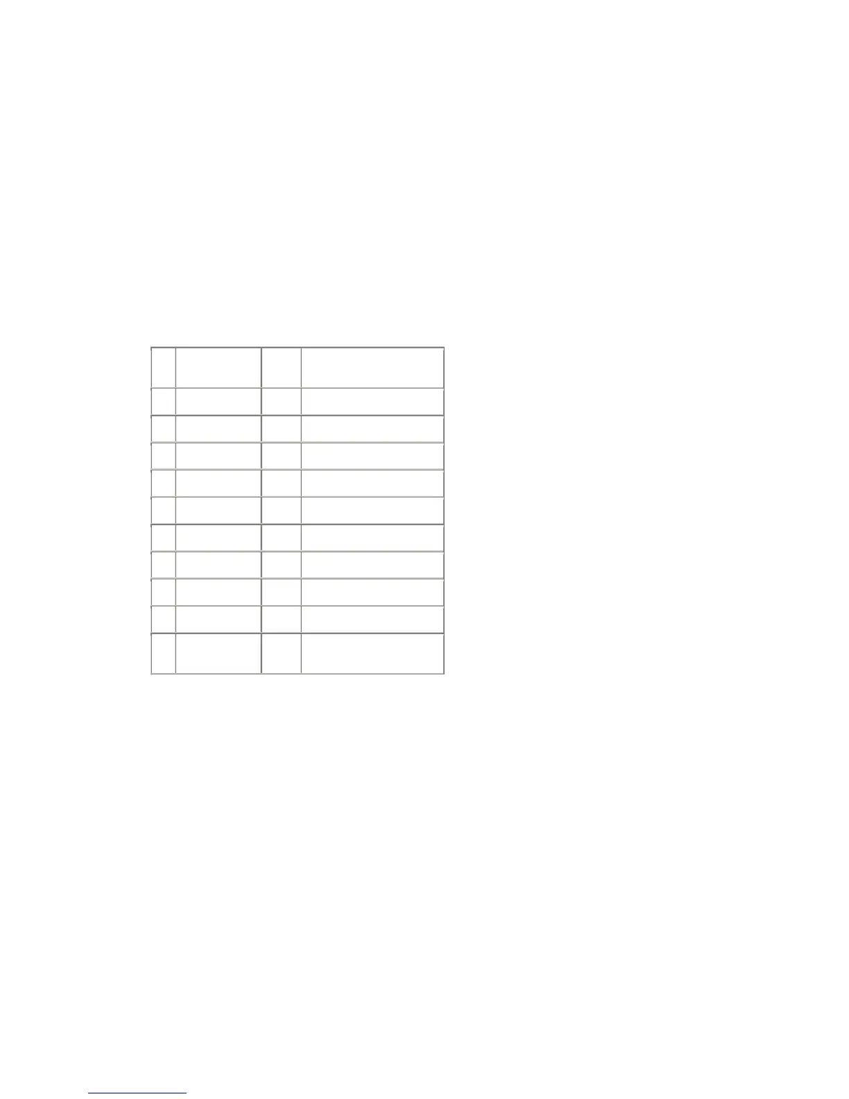
Front Panel Board Connector
PL702
Pin
No.
Pin
Name
In/Out Functions
1 POW LED I Power LED
2 POWER SAVE I POWER2
3 STB+5V I Stand-by 5V power supply
4 GND - GND
5 RM-IN O N.C.
6 A+5V I +5V
7 A/D KEY 2 O Key in 1
8 A/D KEY 1 O Key in 2
9 (BS-LED) - N.C.
10 (MODEM-LED) -
At Front Control
N.C.
4.7. COMB Filter/SVHS Output (Schematic Sheet 6)
CVBS from IC100 pin 26 is filtered by C800, C801, L800, and C802 and connected to pin 3.
Y/C separate signals output from IC101 pin 25/23 are also filtered by Q801 base circuit and Q802
base circuit.
• Y is amplified to adjust the level at Q119/Q120 for return signal to IC100 and SVHS. Y signal
output via buffer Q803.
• C is amplified to adjust the level at Q121/Q122 for return signal to IC100 and SVHS. C signal
output via buffer Q804.
IC101 requires clock at pin 19 supplied from IC100.
4.7.1.
TC9090AF
COMB filter (IC101)
Supply voltage: +5V at pin 15, 18 and 27.
Control by I
2
C: SDA at pin 8 and SCL at pin 9.
 Loading...