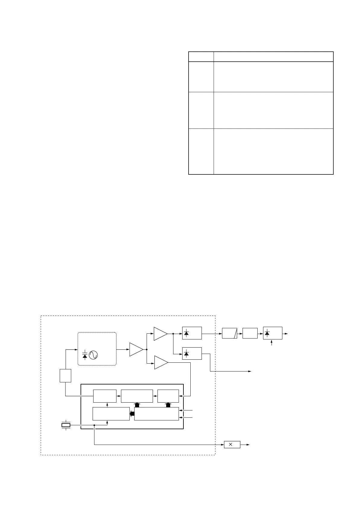
(1) NORMAL OSCILLATING SIGNAL CIRCUIT
The signal from the VCO swtich (D7) passes through the
attenuator (R33, R37, R38, C41) and low-pass filter (L5, L9,
C45, C47, C53, C63, C64), and then applied to the VCO
swtich (D10) which is controlled by the “L_VR5” signal.
(2) TWICE OSCILLATING SIGNAL CIRCUIT
The signal from the VCO switch (D9) passes through the
high-pass (L6, C46, C48, C49), low-pass (L8, C52, C54,
C57) and high-pass (L11, C58, C65) filters to obtain twice
oscillating signal. The signals is applied to the VCO switch
(D11) which is controlled by the “L_UR5” signal.
(3) HARF OSCILLATING SIGNAL CIRCUIT
The signal from the VCO switch (D15) is applied to the pre-
scaler circuit (IC3, pin 2) to divide harf oscillating signal. The
divided signal is applied to the VCO switch (D16).
The reglator circuit provides the pre-scaler’s power supply.
The circuit is controlled by the “L_LO_SW” signal.
The signal from the each VCO switch is applied to the 1st
mixer circuit for right side display (MAIN unit; IC1005, pin 4)
as the 1st LO signal.
A portion of the signal from the buffer amplifier (Q7) is ampli-
fied at the buffer amplifier (Q1), and is then fed back to the
PLL IC (IC1, pin 8) as the comparison signal.
4 - 8
• PLL CIRCUIT FOR LEFT SIDE DISPLAY
Description
The 13.8V external DC power from the power
connector (MAIN unit; J2000). The voltage is
supplied to the LCD back light circuit
(DS1–DS12), etc.
Common 8 V converted from the HV line at the
+8 regulator circuit (Q1, Q3, D1). The output
voltage is applied to the microphone amplifier
regulator circuit (Q16), key back light circuit
(DS13–DS18).
Common 5 V converted from the HV line by the
+5 regulator circuit (CONTROL unit; IC3). The
output voltage is applied to the buffer amplifier
(CONTROL unit; Q2) and reset circuit (CON-
TROL unit; IC2), control unit CPU (IC4) and PTT
detector (Q5, D3, D4).
Line
HV
8V
CPU5
4-4 POWER SUPPLY CIRCUITS
4-4-1 CONTROL UNIT VOLTAGE LINE
 Loading...