4 - 4
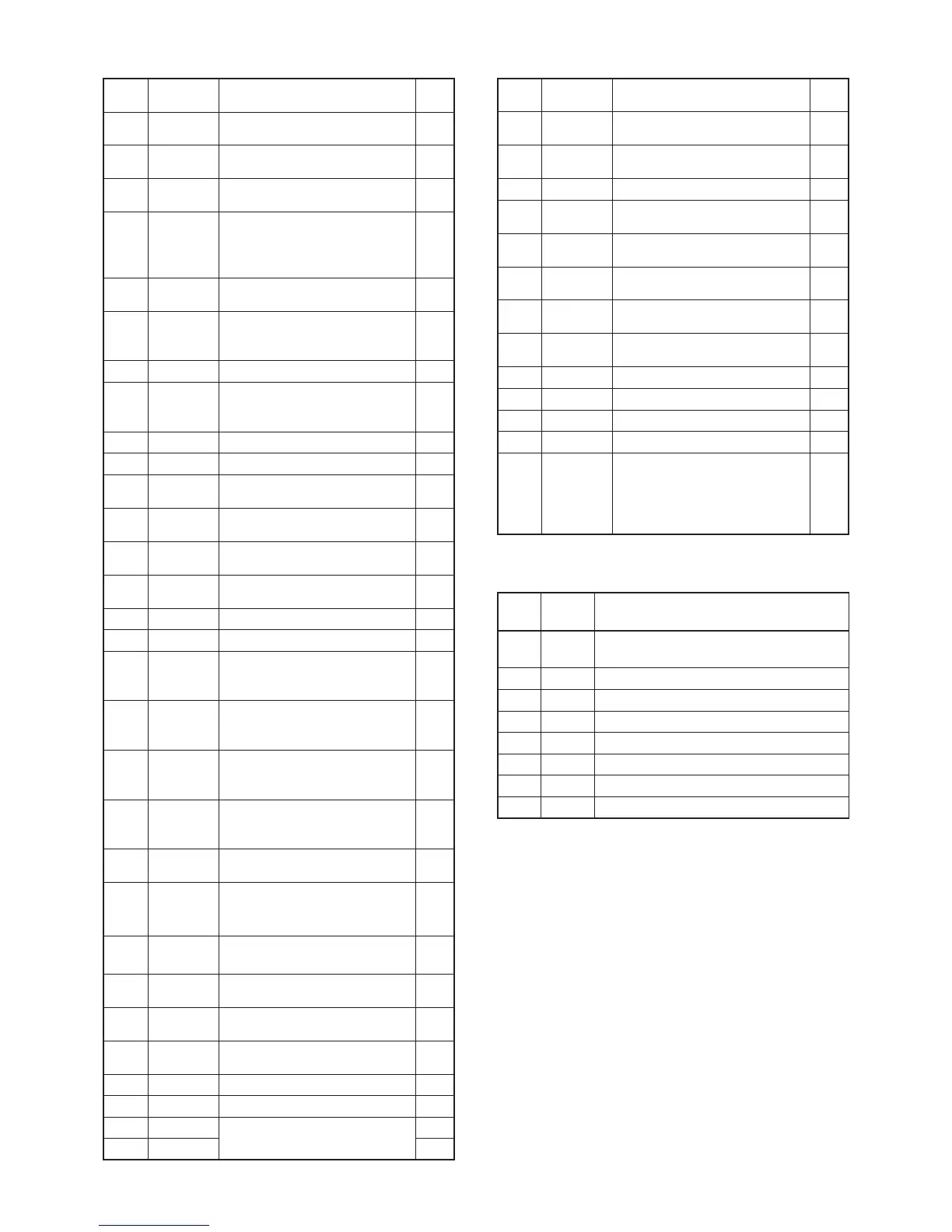
4-5 PORT ALLOCATIONS
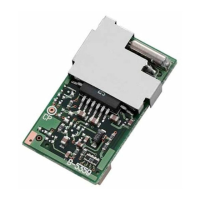
• CPU (IC51)
• D/A CONVERTER (IC57)
PIN
NO.
LINE
NAME
DESCRIPTION
I/O
1 CDEC
Tone signal (CTCSS/DTCS)
decoding input.
I
2 STONE
Tone signal (5/2 TONE, DTMF,
BIIS) decoding/encoding .
I/O
13 CSFT
Clock frequency shift.
H=Clock frequency is shifted.
O
14 NWC
RX mode (narrow/wide)
switching.
L= While receiving in the narrow
mode
O
15 EPTT
External PTT input.
H=An external PTT is pushed.
I
16 ATX
Automatic TX control for VOX
mode.
H=Microphone input is detected.
O
17 BEEP Beep sounds. (Square waves) O
18 AFON
AF power AMP control.
H= AF power AMP (IC55) is
activated.
O
19 SCK Common clock. O
20 SO Common serial data. O
22 KEY2
[UPPER] key input.
L=Pushed
I
23 KEY1
[LOWER] key input.
L=Pushed
I
24 PLST
PLL strobe.
H=Load enable.
I/O
25 DAST
D/A converter strobe.
H=Load enable.
I/O
26 ESDA EEPROM data. I/O
27 ESCL EEPROM clock. I/O
28 R5C
Power supply switching control.
H= Supplying current to the
receiver circuits ("R5"line).
O
29 T5C
Power supply switching control.
H= Supplying current to the
transmitter circuits ("T5"line).
O
30 S5C
Power supply switching control.
H= Supplying current to the RX/
TX common circuits ("S5"line).
O
31 PWON
Power supply switching control.
H= The transceiver's power is
ON.
O
32 IPTT
Internal PTT input.
L=PTT pushed.
I
33,
34,
36
CENC2,
CENC1,
CENC0
CTCSS/DTCS signal. O
37–
40
CBI0–
CBI3
[ROTARY SELECTOR] input. I
41 DUSE
Frequency response switching.
H=DTCS encoding
O
42 RLED
Busy LED (Green) control.
L=LED lights
. (Squelch open)
O
43 TLED
Busy LED (Red) control.
L=LED lights. (Transmit)
O
47 MGC0 MIC gain control. O
48 MGC1 MIC gain control. O
49 CLI
Cloning data.
I
50 CLO O
PIN
NO.
LINE
NAME
DESCRIPTION
I/O
51 ADSW
A/D conversion select.
H=RSSI input, L=BATV input
O
53 NOIS
Noise level detect.
H=Squelch close
I
54 UNLK PLL unlock detect. I
55 RMUT2
RX AF mute switch control.
L=AF mute.
O
56 RMUT1
RX AF mute switch control.
L=AF mute.
O
57 MMUT
MIC mute switch control.
L=MIC mute.
O
58 TMUT
Transmission mute.
L=TX inhibit.
O
59 MDET
External microphone connection
detect.
I
60 LVIN Lock voltage input. I
61 TEMP Temperature sensing voltage. I
62 AFVI [VOLUME CONTROL] input. I
63 VOXV
Microphone input sensing voltage.
I
64 AD5
Remaining battery voltage.
(or)
RSSI voltage.
( The input signal depends on the
status of pin 51.)
I
PIN
No.
LINE
NAME
DESCRIPTION
23 T1
(TXPO)
BPF tuning voltage
TX power control
24 T2 BPF tuning voltage
7 REF Reference frequency adjust voltage.
8 LVA Additional lock voltage adjustment.
11 SQLC Squelch threshold setting.
12 TENC CTCSS deviation adjustment.
19 BAL DTCS balance.
20 VRAF Max. deviation/AF volume adjustment.
 Loading...