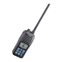
4 - 4
4-5 PORT ALLOCATIONS
• CPU (IC360)
• D/A CONVERTER (IC190)
PIN
No.
LINE
NAME
DESCRIPTION I/O
1 BEEP Beep audio (Squarewave). O
2 PS PLL power save mode control. O
3 TDEC
Decoded tone signal. (for monitoring
purpose)
O
4 DASTB Strobe for the D/A converter. O
5 PLSTB Strobe for the PLL IC. O
10 SDATA
Serial data for the PLL IC and D/A
converter.
O
11 SCK
Serial clock to the PLL IC and D/A
converter.
O
12 ESCK Serial clock for the EEPROM. O
13 ESDA Serial clock from/to the EEPROM. I/O
25 RES CPU reset. I
27 TEMPV Temparature sensing voltage. I
28 BTEMPV Battery temparature sensing voltage. I
29 LOINV Lock voltage from the PLL IC. I
30 TDETV TX power sensing voltage. I
31 BATTV Battery voltage. (Divided voltage) I
32 RSSIV
RSSI voltage from the IF demodulate IC.
I
33 NOISV
Noise level sensing voltage from the
IF demodulate IC.
I
34 DCV Input voltage detection. I
36 WDECV* Weather alart tone signal. I
38 ATIS** ATIS signal. O
51–
72
SEG0-
SEG21
LCD driver segment terminals. O
77 LEDS Backlight control. O
78 CRESET Charging control IC reset. O
79 LCDS LCD contrast control. O
80 MICMS
MIC mute SW control.
L=MIC mute.
O
81 ATX
MIC control.
H=While transmitting.
O
85 AFVS
AF power AMP control.
H=While the squelch is opened.
O
86 V3VS VCO power supply control. O
87 M3VS Main power supply control. O
88 LOW
TX power control.
H=The TX power is set to Low.
O
89 R3VS
R3V line control.
L= While receiving. (RX circuits
activated)
O
90 T3VS
T3V line control.
L= While transmitting. (TX circuits
activated)
O
97 PON Main power supply line control. O
98 DETMS
RX AF line mute.
L=Mute.
O
99 LEDI-R
Charge status.
L=While charging.
Pulse=Charging error.
I
100 LEDI-G
Charge status.
L=When the battery is fully charged.
I
*: M24 only **: [FRG] and [HOL] only
PIN
No.
LINE
NAME
DESCRIPTION I/O
101 PTTM
MIC mute control.
L=MIC mute.
O
103 PTTIN
[PTT] input.
H=Pushed.
I
106 LOW
TX power control.
H=TX power is set to low.
O
107 TXMS
Transmitting control.
H=TX mute.
O
108 16/9
[16/9] input.
L=Pushed.
I
109 CH/WX
[CH/WX] input.
L=Pushed.
I
110 UP
[
Y
] input.
L=Pushed.
I
111 DOWN
[
Z
] input.
L=Pushed.
I
112 FAV
[FAV] input.
L=Pushed.
I
113 VOL/SQL
[VOL/SQL] input.
L=Pushed.
I
114 SCAN
[SCAN] input.
L=Pushed.
I
116 H/L
[H/L] input.
L=Pushed.
I
117 UNLK
PLL unlock signal input. (PLL
malfunction detection)
H=PLL unlocked.
I
119 PWSW
[
] input.
H=Pushed.
I
PIN
No.
LINE
NAME
DESCRIPTION
1, 2 FCON Reference frequency adjustment voltage.
3, 4 PCON TX output power adjustment voltage.
9, 10 MODC Deviation adjustment.
11, 12 MSENS
MIC signal level (MIC sensitivity) adjustment.
13, 14 VOLO AF output power adjustment.
15, 16 SQLO Squelch threshould level adjustment.
21, 22 T1CON BPF tuning voltage.
 Loading...