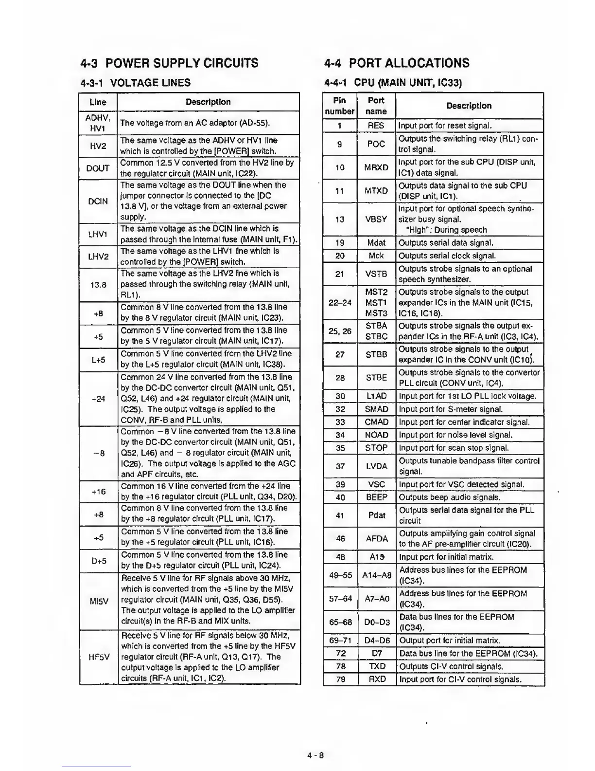
4-3
POWER SUPPLY CIRCUITS
4-3-1
VOLTAGE LINES
Line
Description
ADHV.
HV1
The
voltage from an AC
adaptor
(AD-55).
HV2
The same
voltage
as the
ADHV or
HV1 line
which Is
controlled
by
the
(POWER)
switch.
DOUT
Common 12.5 V
converted
from the HV2
line
by
the regulator circuit
(MAIN unit,
IC22).
DCIN
The same
voltage
as the
DOUT line when the
jumper
connector
Is
connected to the
[DC
1
3.8 V], or the voltage from an external power
supply.
LHV1
The same
voltage
as
the DCIN line
which
is
passed
through the Internal fuse (MAIN unit, FI).
LHV2
The same
voltage
as the
LHVI line
which is
controlled by the (POWER) switch.
13.8
The
same
voltage
as
the LHV2
line which is
passed through
the switching relay (MAIN unit,
RL1).
+8
Common 8
V line converted from the 1 3.8
line
by the
8
V regulator circuit (MAIN unit, IC23).
+5
Common
5
V line
converted from
the 13.8 line
by the
5
V regulator circuit (MAIN unit,
IC17).
L+5
Common 5 V line
converted from the LHV2 line
by the L+5
regulator circuit
(MAIN
unit. IC38).
+24
Common 24 V line converted
from
the 13.8
line
by
the
DC-DC
convertor circuit
{MAIN unit,
Q51
.
Q52,
L46)
and
+24 regulator
circuit
(MAIN unit,
IC25).
The output voltage is applied to the
CONV, RF-B and PLL
units.
-8
Common
-8
V
line converted from the
13.8
line
by the DC-DC
convertor circuit (MAIN unit,
Q51
,
Q52, L46) and
-
8
regulator circuit (MAIN unit,
IC26).
The output voltage is applied to the AGC
and APF circuits, etc.
+16
Common
1 6
V line converted from the +24 line
by the
+16 regulator circuit (PLL unit,
Q34,
D20).
+8
Common
8
V line converted from the
13.8
line
by
the +8 regulator
circuit
(PLL
unit.
IC17).
+5
Common
5
V line converted from the 1 3.8 line
by
the +5
regulator circuit
(PLL
unit.
IC16).
D+5
Common 5
V line converted
from
the
1 3.8
line
by
the
D+5
regulator circuit
(PLL
unit,
1C24).
MI5V
Receive
5
V line tor RF signals above
30
MHz,
which is
converted from
the
+5 line by
the MI5V
regulator
circuit
(MAIN unit,
Q35. Q36,
D55).
The
output voltage Is applied
to the LO
amplifier
circuit(s) in the RF-B and MIX units.
Hf5V
Receive
5
V line for RF signals below
30
MHz.
which is
converted
from the +5 line by the HF5V
regulator circuit (RF-A
unit.
Q13, Q17).
The
output voltage Is applied
to
the
LO
amplifier
circuits (RF-A unit, IC1
,
IC2).
4-4
PORT ALLOCATIONS
4-4-1
CPU
(MAIN UNIT,
IC33)
Pin
number
Port
name
Description
1 RES Input port for
reset
signal.
9 POC
Outputs
the switching relay
(RL1
)
con-
trol
signal.
10 MRXD
Input port for
the
sub
CPU (DISP unit,
IC1) data
signal.
11
MTXD
Outputs data
signal
to
the
sub CPU
(DISP unit, IC1).
Input port for
optional
speech synthe-
13
VBSY sizer busy signal.
"High"
: During speech
19
Mdat
Outputs serial data signal.
20
Mck Outputs serial clock signal.
21 VSTB
Outputs strobe signals to an optional
speech synthesizer.
MST2 Outputs strobe signals to the output
22-24
MST1 expander ICs in the
MAIN
unit (IC15,
MST3 IC16, IC18).
25.
26
STBA
Outputs
strobe signals the
output ex-
STBC pander ICs In the RF-A unit
(ICS,
IC4).
27 STBB
Outputs
strobe signals
to
the
output^
expander 1C in the CONV unit (ICIO).
28
STBE
Outputs strobe signals
to
the convertor
PLL
circuit
(CONV unit.
IC4).
30 L1AD
Input port
for
1st LO
PLL lock voltage.
32 SMAD Input port for S-meter signal.
33
CMAD
Input port
for
center indicator signal.
34
NOAD Input port for noise level signal.
35
STOP Input port for scan stop signal.
37 LVDA
Outputs
tunable bandpass filter
control
signal.
39
VSC Input port for VSC detected signal.
40 BEEP Outputs beep audio signals.
41 Pdat
Outputs serial data signal for the PLL
circuit
46
AFDA
Outputs
amplifying
gain
control
signal
to the AF pre-amplifier circuit (IC20).
48 A15 Input port for initial matrix.
49-55
A14-A8
Address bus lines for the
EEPROM
(IC34).
57-64
A7-A0
Address bus lines for the
EEPROM
(1C34).
65-68
DO-D3
Data bus
lines for
the EEPROM
(IC34).
69-71
D4-D6 Output
port
for initial matrix.
72
D7 Data bus line for the EEPROM
(1C34).
78 TXD Outputs Cl-V control
signals.
79 RXO Input port for Cl-V control signals.
4-8
 Loading...