4 - 3
4-2-4 APC CIRCUIT (1F AND 2F UNITS)
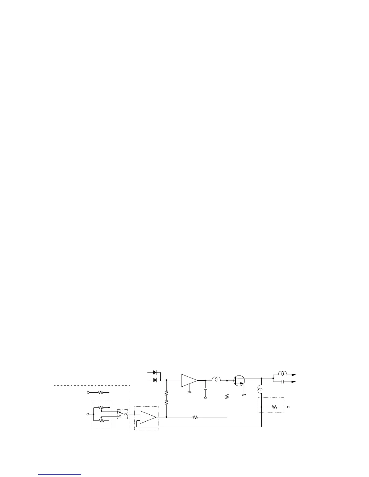
The APC circuit stabilizes transmit output power and selects
HIGH and LOW output power. The APC circuit consists of
APC sensor, APC control (1F unit) and APC set (2F unit) cir-
cuits.
The APC sensor circuit (1F unit; R250) detects a driving cur-
rent from a drive voltage at the PA board. The detected cur-
rent is applied to the ope-amplifier IC (1F unit; IC250, pin 2)
in the APC control circuit, and compared with a “PSET” volt-
age which is supplied from the APC set circuit (2F unit;
IC301). The output voltage from pin 1 of IC250 is applied to
the APC control circuit (1F unit; Q255 base) to control
“VGGC” voltage.
The “VGGC” APC control signal is separated for VHF
(VGG1) and UHF (VGG2) by resistors. The VGG1 line is for
the APC control signal for the drive amplifier and the VGG2
line is for the power amplifier.
Low output power is obtained by changing the “PSET” volt-
age coming from pin 1 of IC301 on the 2F unit. The “PSET”
voltage is controlled by power set pots (2F unit; R302 for
VHF, 2F unit; R304 for UHF) and an “H/L” signal via the CPU
(LOGIC unit; IC1, pin 56). A thermistor (R266) controls APC
reference voltage (“PREF” voltage) to reduce the output
power when the temperature is increased.
4-2-5 ANTENNA SWITCHING CIRCUIT
(1F UNIT)
The antenna switching circuit applies receive signals to the
receiver circuit and transmit signals to the antenna connec-
tor.
(1) VHF ANTENNA SWITCHING CIRCUIT
When transmitting, D51 D52 and D202 are turned ON. The
signal passes through the low-pass filter (L10–L12,
C16–C22) and is then applied to the antenna connector. The
low-pass filter suppresses high harmonic components.
(2) UHF ANTENNA SWITCHING CIRCUIT
When transmitting, D722-D724, D551, D552 and Q204 are
turned ON. The signal passes through the low-pass (L7–L9,
C9–C15) and high-pass (L1–L3, C1–C5) filters and is then
applied to the antenna connector. The high-pass filter sup-
presses low harmonic components.
4-3 PLL CIRCUITS
4-3-1 VHF PLL CIRCUIT (1F UNIT)
The oscillated signal at the VCO circuit (DUAL VCO board;
Q304, Q305 and D303) is amplified at a buffer-amplifier
(Q306) and is again amplified at another buffer-amplifier
(Q352). The amplified signal is applied to the PLL IC (IC851,
pin 2), and then divided by serial data from the CPU and
phase-detected with the divided reference frequency. The
phase difference is output as pulses.
The output signals from IC851 (pin 8) are converted to DC
voltages (lock voltage) by the loop filter (R366–R368, C362,
and C364) and are then fed back to the VHF VCO circuit to
stabilize the VCO frequency.
The DC voltage is also applied to the receiver tuned band-
pass filters as a “VTUNE” signal.
4-3-2 UHF PLL CIRCUIT (1F UNIT)
The oscillated signal at the VCO circuit (DUAL VCO board;
Q301, Q302, D301 and D302) is amplified at a buffer-ampli-
fier (Q306) and is again amplified at another buffer-amplifier
(Q352). The amplified signal is applied to the PLL IC (IC851,
pin 19), and then divided by serial data from the CPU. It is
the phase-detected with the divided reference frequency
and the phase difference is output as pulses.
The output signals from IC851 (pin 13) are converted to DC
voltages (lock voltage) by the loop filter (R866–R868, C862
and C864) and are then fed back to the UHF VCO circuit to
stabilize the VCO frequency.
 Loading...