Application Note 10 2011-07-06
2==
n
N
N
p
s
2.2.8 SR MOSFET
The voltage stress on the drain-source of the MOSFET is:
VVVV
fods
2.242*)( =+=
The RMS value of the current flowing through each MOSFET is:
AII
ormsd
63.19
4
_
==
2.3 Design of Control Parameters and Protections
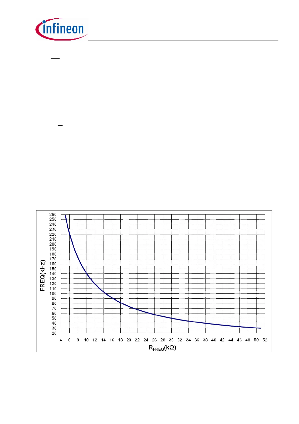
2.3.1 Frequency setting:
The IC internal circuit provides a regulated 2V voltage at FREQ pin. The effective resistance presented
between the FREQ pin and GND, determines the current flowing out of the FREQ pin, which in turn
defines the switching frequency.
Figure 3 shows the curve illustrating the relationship of Switching Frequency
FREQ Vs Effective
Resistor
FREQ
R connected between the FREQ pin and gound.
Figure 3
FREQ
Vs Effective Resistor
FREQ
R
2.3.2 Minimum/Maximum frequency setting:
 Loading...