SECTION
IV
THEORY OF
OPERATION
The
following
descriptions
of the
circuitry
in the
amplifier are presented
so
the
professional
user
may
have
a
general
understanding
of how the
amplifier works. They
are
not
intended as
a
guide
for
service.
Service on
this product should be
performed
only
by
qualified
technicians.
THERE ARE
NO USER
SERVICEABLE PARTS INSIDE. In
the
following
descriptions the
component
designations
for Channel A are used. Examination
of the
accompanying
schematic
will aid
in
understanding
the following circuit
descriptions.
4.1
INPUT DIFFERENTIAL AMPIIFIEB
The
input
differential
amplifier
is
comprised of
IC1
C
and D and associated
components.
Input
signals are coupled
to
the
amplifier after passing through one of three
connector
types
and
passing across
RF
suppression
capacitors.
Two
amplifier sections
are used
as
unity
gain inverters with the
output
of one
summed to
the
Input of
the other to
improve
common mode cancellation.
Signals which
appear
equally on both
Input
terminals,
such as
common mode
noise arid hum,
will
be
cancelled. Use
of the
Inverting mode
in
both
sections assures
high
speed, good
common
mode
rejection and equal
impedance
at
both
input terminals.
This gives
a
substantial
advantage
over less
expensive
single
amplifier topologies.
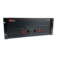
4.2
MODE SWITCH
The rear panel mode
switch
allows
the
amplifier
to
operate
in
the Stereo, Dual
Mono
or
Bridged Mono
modes. In the
Stereo
mode, each
channel operates normally. In
the
Dual Mono,
Channel A
input is routed to
both
Channel A
and
B
differential
amplifiers.
In the
Bridged
Mono mode, the
Channel A
input
goes to
the Channel A
differential
amplifier, and
is simultaneously
inverted
via the mode
switch and
fed
to
the Channel B
differential
amplifier.
Bridging the
load across
outputs A and
B results
in
twice the
voltage
across the load
and
four times
the
power
as
compared
to
one
channel
driven
into the
same
load.
The
minimum load
impedance
in this
configuration is
8
ohms.
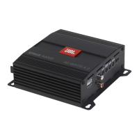
4.3
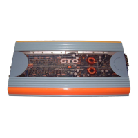
POWERAMPLIFEB
The
JBL/UREI Model 6290
Power
Amplifier
employs discrete transistor
circuitry in
the
voltage
amplifier and output
stage.
A
symmetrical topology
was chosen
to
take
advantage
of
distortion
cancellation
effects
and equal
group delay
for
each
half of the
signal.
This allows
simple
compensation,
exceedingly wide open-loop
frequency
response
and
excellent
transient
Intermodulation
performance.
Q20-23 are
configured
in matching
differential amplifiers
loaded by
the
emitters of
Q7
and Q9.
Note that
no
inverting
amplifiers
are
used.
All
transistors are used
in current-
mode,
non-inverting
connections.
This eliminates
bandwidth
limiting
due to
Miller
effect
(the
effective
multiplication of
collector-base
capacitance
by
voltage
gain), and
resultant
reduction of
high frequency response.
Looking at the lop half" of
Channel A, Q23
functions
as
an
emitter follower
driving Q22
In the common
base mode.
The feedback
signal
at
R37
is
subtracted
from the Input
at
this point. Collector current
from Q22 is
cascode
connected to
the emitter
of
Q7,
which Is also common base connected.
Q7
IV-1
 Loading...