2-2
2.2 CCD (ICX220AK/ICX221BK)
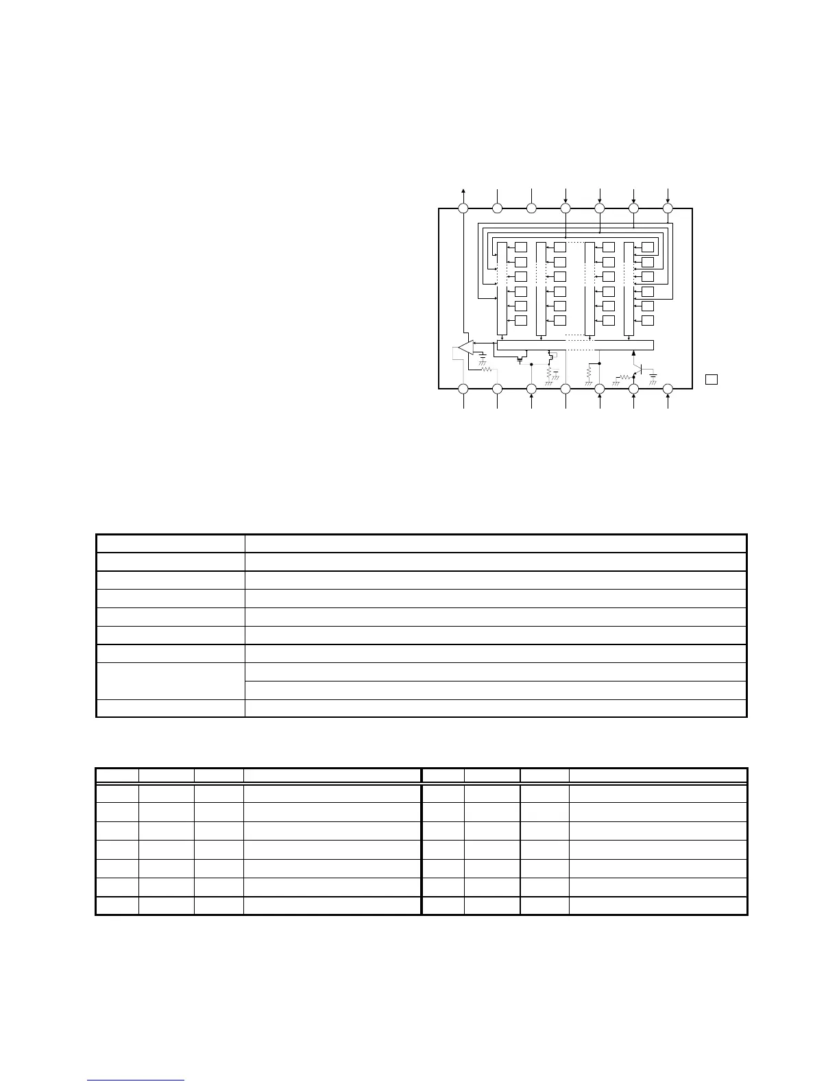
This IC functions as an interline CCD (Charge
Coupled Device = one of solid-state pickup
devices). Since this CCD conforms to the SD
mode of the DV standard, it has an optimum
number of vertical pixels for the MPEG2 main level
and it realizes a horizontal resolution of 450 TV
lines. As same as general CCD's currently in use,
this CCD is capable of camera shaking correction
and electronic panning and tilting owing to the
extension area of 33 percent extra in both the
vertical and horizontal directions.
Moreover, this CCD provides high quality wide
picture whose aspect ratio is exactly 16:9 without
vertical interpolation.
High sensitivity and low dark current are realized
thanks to adoption of the Super HAD CCD
technology with the color filters of yellow, cyan,
magenta and complementary green mosaic filters.
This CCD has an electronic shutter function that is
able to vary charge storage time by the field period
read system.
Frame period read system is realized by joint use
of the newly developed TG IC.
HØ1
HØ2
ØRG
ØSUB
VØ1
VØ2
VØ3
VDD
Photo
Sensor
VØ4
1
Ye
G
Ye
Mg
Ye
G
Cy
Mg
Cy
G
Cy
Mg
Ye
G
Ye
Mg
Ye
G
Horizontal-Register
Vertical-Register
14131211108 9
7 6 5 4 3 2
GND
VOUT
TEST
∗
Cy
Mg
Cy
G
Cy
Mg
GND
VL
∗
Fig. 2-2-1 CCD block diagram
ELEMENT STRUCTURE Interline type CCD image sensor
Optical size 1/4 inch size format
Total pixels NTSC: 998 (H) × 677 (V) approx. 680,000 pixels, PAL: 998×797 approx. 800,000 pixels
Effective pixels NTSC: 962 (H) × 654 (V) approx. 630,000 pixels, PAL: 962×774 approx. 740,000 pixels
4:3 NTSC NTSC: 711 (H) × 485 (V) approx. 340,000 pixels, PAL: 702×575 approx. 400,000 pixels
16:9 18MHZ NTSC: 948 (H) × 485 (V) approx. 460,000 pixels, PAL: 936×575 approx. 540,000 pixels
16:9 5fsc NTSC: 942 (H) × 485 (V) approx. 460,000 pixels, PAL: 922×575 approx. 530,000 pixels
H direction: Front 4 pixels, Rear 32 pixels
V direction: Front 11pixels, Rear 12 pixels
Board material Silicon
OB
Table 2-2-1 CCD functions
Pin No. Label In/Out Description Pin No. Label In/Out Description
1
V
φ
4
In Vertical register transfer clock 8 VOUT Out Video signal output
2
V
φ
3
In Vertical register transfer clock 9 GND - Ground
3
V
φ
2
In Vertical register transfer clock 10
φ
RG
In Reset gate clock
4
V
φ
1
In Vertical register transfer clock 11
H
φ
1
In Horizontal register transfer clock
5 GND - Ground 12
H
φ
2
In Horizontal register transfer clock
6 TEST - Open 13
φ
SUB
In Substrate clock
7 VDD - Power supply 14 VL - Protect transistor bias
Table 2-2-2 CCD pin function
 Loading...