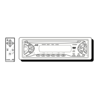
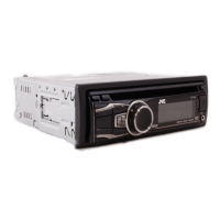
KD-S595
(No.49768)1-35
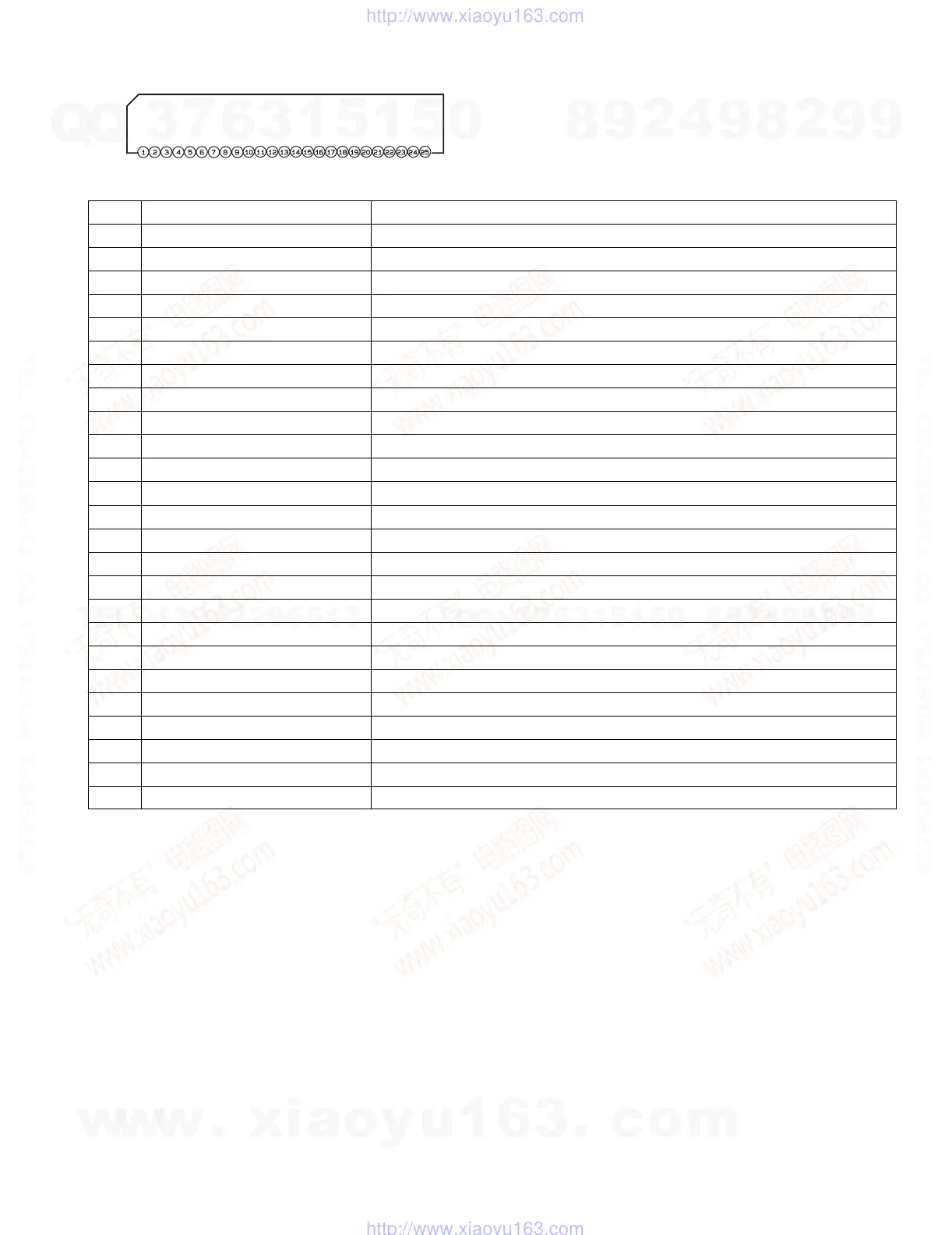
•Pin layout
• Pin function
TAB
GND
FR-
STDBY
FR+
VP1
RR-
GND
RR+
RIPPLE
INRF
INRR
SGND
FLIN
RLIN
DNTIME
RL+
GND
RL-
VP3
FL+
MUTE
FL-
GND
NC
Pin No. Symbol Function
1 TAB Header of IC
2 GND Power GND
3 FR- Outpur(-) for front Rch
4 STDBY Stand by input
5 FR+ Output (+) for front Rch
6 VP1 Power input
7 RR- Output (-) for rear Rch
8 GND Power GND
9 RR+ Output (+) for rear Rch
10 RIPPLE Ripple filter
11 RRIN Rear Rch input
12 FRIN Front Rch input
13 SGND Signal GND
14 FLIN Front Lch input
15 RLIN Rear Lch input
16 ONTIME Power on time control
17 RL+ Output (+) for rear Lch
18 GND Power GND
19 RL- Output (-) for rear Lch
20 VP3 Power input
21 FL+ Output (+) for front
22 MUTE Muting control input
23 FL- Output (-) for front
24 GND Power GND
25 NC Non connection
w
w
w
.
x
i
a
o
y
u
1
6
3
.
c
o
m
Q
Q
3
7
6
3
1
5
1
5
0
9
9
2
8
9
4
2
9
8
T
E
L
1
3
9
4
2
2
9
6
5
1
3
9
9
2
8
9
4
2
9
8
0
5
1
5
1
3
6
7
3
Q
Q
TEL 13942296513 QQ 376315150 892498299
TEL 13942296513 QQ 376315150 892498299
http://www.xiaoyu163.com
http://www.xiaoyu163.com
 Loading...