1-32
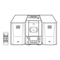
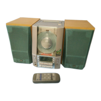
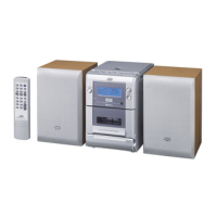
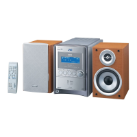
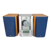
UX-V30
30
29
28
27
26
25
24
23
22
21
20
19
18
17
16
15
14
13
12
11
10
9
8
7
6
5
4
3
2
1
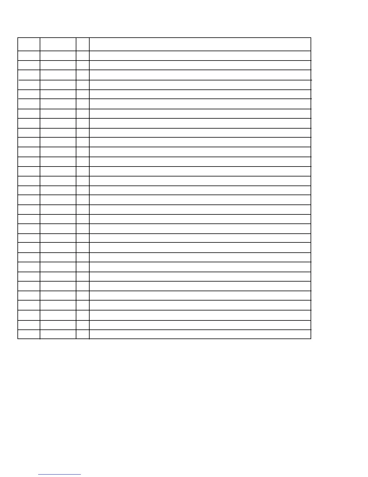
3. Pin function
Pin No.
symbol
I/O
I
O
I
--
I
O
I
I
O
I
I
I
I
--
O
I
O
I
I
Function
D1
CE
Serial data input pin for control
Chip enable pin
Vss Ground
TEST
TEST pin for electronic volume control
LOUT Volume+equalizer output
LBASS2
Bas-band filter comprising capacitor and resistor connection
LBASS1
Bas-band filter comprising capacitor and resistor connection
LTRE
I
Capacitor connection pin comprising treble band filter
LIN
Volume+equalizer intput
LSEL0 Input selector output pin
L4
Input signal pin
L3
Input signal pin
L2
Input signal pin
L1
Input signal pin
NC
No connect
NC
--
No connect
R1
Input signal pin
R2
R3
R4
I
I
I
Input signal pin
Input signal pin
Input signal pin
RSEL0
Input selector output pin
RIN
Volume+equalizer intput
RTRE
Capacitor connection pin comprising treble band filter
I
I
RBASS1
Bas-band filter comprising capacitor and resistor connection
I
RBASS2
Bas-band filter comprising capacitor and resistor connection
ROUT
O
Volume+equalizer output
NC
-- No connect
Vref
O
Analog ground
VDD
Poer Supply
CL Clock input
 Loading...