- 13 -
(12) Choose the Hex file in folder and execute downloading
with click “open button”.
(13) Click OK button at the “edit window”.
(14) Under Downloading progress.
(15) If download is failed, for example “No acknowledge from
slave”, execute download again from (1).
4. Channel memory download
(1) Push the NVM button.
(2) Push the button change and select the Channel memory
data.
(3) Push the Update NVM from File.
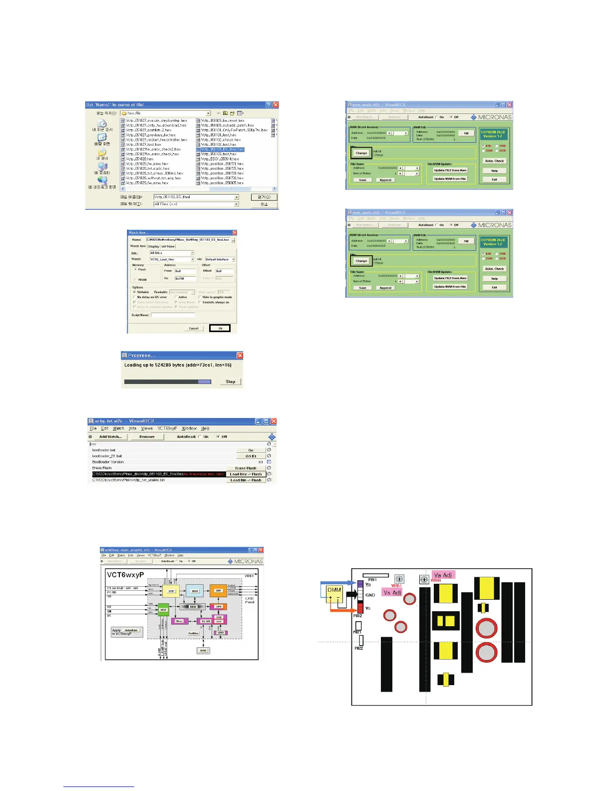
5. POWER PCB Assy Voltage
Adjustments
(Va, Vs Voltage adjustments)
5-1. Test Equipment : D.M.M. 1EA
5-2.Connection Diagram for Measuring
: refer to Fig.1
5-3. Adjustment Method
(Power board - P/N : 6709900019A)
(1) Va Adjustment
1) After receiving 100% Full White Pattern, HEAT RUN.
2) Connect + terminal of D. M..M. to Va pin of P812,
connect -terminal to GND pin of P812.
3) After turning RV901,voltage of D.M.M adjustment as
same as Va voltage which on label of panel right/top.
(deviation; ±0.5V)
(2) Vs Adjustment
1) Connect + terminal of D.M..M. to Vs pin of P851,
connect -terminal to GND pin of P812.
2) After turning RV 951, voltage of D.M.M adjustment as
same as Vs voltage which on label of panel right/top.
(deviation ; ±0.5V)
(Fig. 1) Connection diagram of power adjustment for measuring.

 Loading...