2-14
INTERNAL BLOCK DIAGRAM OF ICs
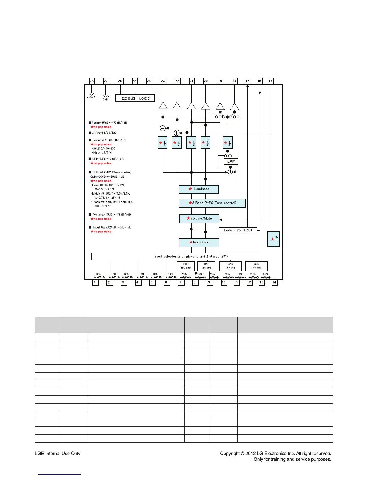
1. IC601 (BD3702FV)
1-1. BLOCK DIAGRAM
1-2. PIN DESCRIPTION
Terminal Terminal
Description
No. Name
1 A1 A input terminal of 1ch
2 A2 A input terminal of 2ch
3 B1 B input terminal of 1ch
4 B2 B input terminal of 2ch
5 C1 C input terminal of 1ch
6 C2 C input terminal of 2ch
7 DP1 D positive input terminal of 1ch
8 DN D negative input terminal
9 DP2 D positive input terminal of 2ch
10 EP1 E positive input terminal of 1ch
11 EN1 E negative input terminal of 1ch
12 EN2 E negative input terminal of 2ch
13 EP2 E positive input terminal of 2ch
14 MIN Mixing input terminal
Terminal Terminal
Description
No. Name
15 MUTE External compulsory mute terminal
16 LRST Level meter reset terminal
17 LOUT Output terminal for Level meter
18 OUTS2 Subwoofer output terminal of 2ch
19 OUTS1 Subwoofer output terminal of 1ch
20 OUTR2 Rear output terminal of 2ch
21 OUTR1 Rear output terminal of 1ch
22 OUTF2 Front output terminal of 2ch
23 OUTF1 Front output terminal of 1ch
24 VCC Power supply terminal
25 SCL I
2
C Communication clock terminal
26 SDA I
2
C Communication data terminal
27 GND GND terminal
28 FIL VCC/2 terminal
 Loading...