Interfaces
RF and baseband interfaces
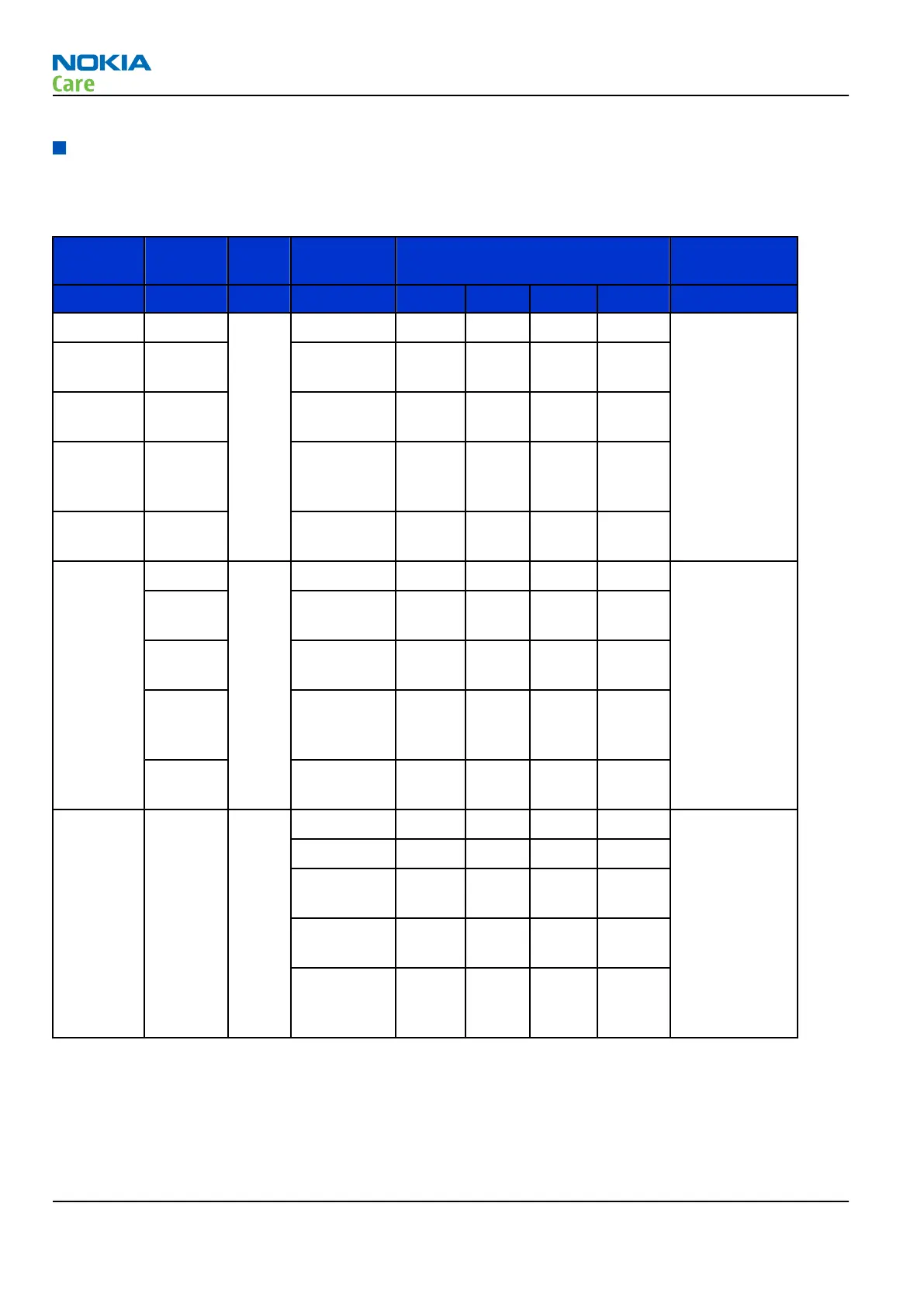
Table 8 AC and DC Characteristics of BB4.0 LiteV2 RF-Base band Digital Signals
Signal
name
From To Para-meter Input characteristics Function
Min Typ Max Unit
TXP1 UPP RF-IC 1 1.38 1.88 V Depends of
the RF design
RFGenOu
t3
GenIO5 0 0 0.4 V
Load
Resistance
10 kW
Load
Capacitanc
e
20 pF
Timing
Accuracy
¼ symbo
l
TXP2 UPP RF-IC 1 1.38 1.88 V Depends of
the RF design
(GenIO6
)
0 0 0.4 V
Load
Resistance
10 kW
Load
Capacitanc
e
20 pF
Timing
Accuracy
¼ symbo
l
RFBusEn1
X
UPP RF-IC 1 1.38 1.88 V RFIC Chip SelX
0 0 0.4 V
Internal PU
Current
50 uA
Load
resistance
10 kW
Load
capacitanc
e
20 pF
RM-340; RM-341
System Module
Page 6 –12 COMPANY CONFIDENTIAL Issue 1
Copyright © 2007 Nokia. All rights reserved.
 Loading...