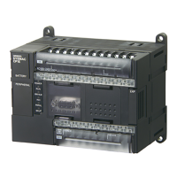
CS/CJ Series HOST Link Driver
GP-Pro EX Device/PLC Connection Manual
35
6 Supported Device
Range of supported device address is shown in the table below. Please note that the actually supported range of
the devices varies depending on the External Device to be used. Please check the actual range in the manual of
your External Device.
This address can be specified as system data area.
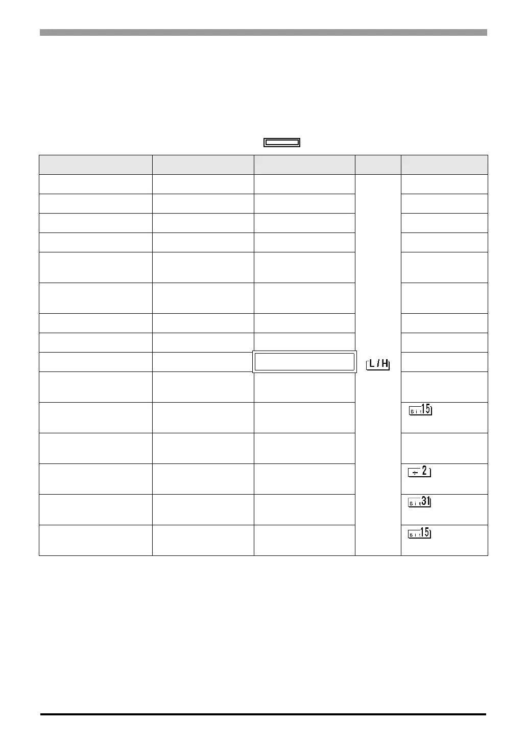
Device Bit Address Word Address 32bits Notes
Channel I/O 0000.00-6143.15 0000-6143
Internal Auxiliary Relay W000.00-W511.15 W000-W511
Special Auxiliary Relay A000.00-A959.15 A000-A959
*1
*1 Write disable in A000 to A447.
Latch Relay H000.00-H511.15 H000-H511
Timer
(Time Up Flag)
T0000-T4095 -
*2
*2 Write disable
Counter
(Count Up Flag)
C0000-C4095 -
*2
Timer (Current Value) - T0000-T4095
Counter (Current Value) - C0000-C4095
Data Memory D00000.00-D32767.15 D00000-D32767
*3
*3 When using the communication unit (CS1W-SCU21), do not use the address of D30000 to D31599. When using
the communication board (CS1W-SCU21/41), do not use the address of D32000 to D32767. These addresses
may be used as the system setting area on the External Device.
Extension Data Memory
(E0-EC)
E000000.00-
EC32767.15
E000000-EC32767
*4*5
*4 Max 13 banks (E0 to EC) can be used. 1 bank can contain 32768 words. Available bank number is different
depending on the CPU unit.
*5 CJM1 Series does not include the extension data memory (E0 to EC, current bank EM).
Extension Data Memory
(Current Bank)
- EM00000-EM32767
*5*6
*6 CJ Series does not include the extension data memory (current bank EM).
Task Flag
(Bit)
TKB00-TKB31 -
*2
Task Flag
(Status)
TK00.00-TK31.07 TK00-TK30
*2
Index Register - IR00-IR15
*7
*7 You cannot write during RUN.
Data Register - DR00-DR15
*7
 Loading...