GSM/GPRS Module Series
M66 Hardware Design
M66_Hardware_Design Confidential / Released 24 / 80
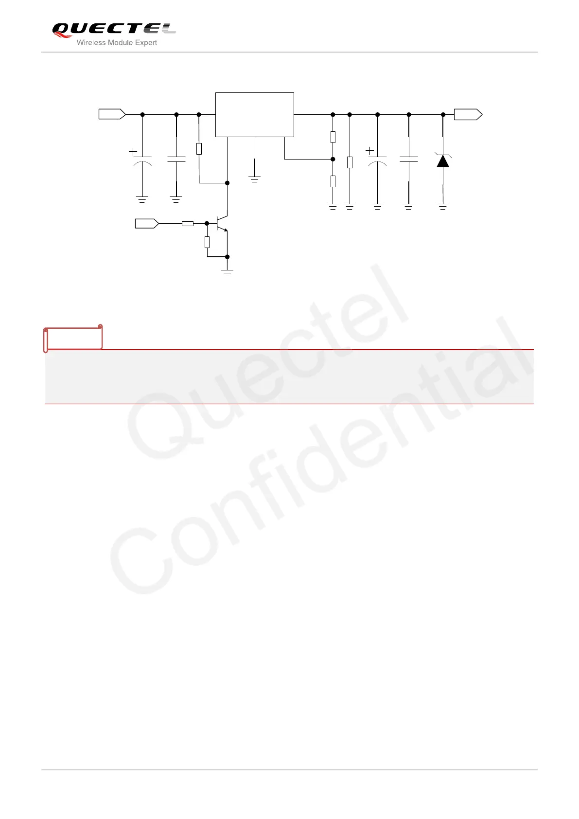
DC_IN
C1
C2
MIC29302WU U1
IN OUT
EN
GND
ADJ
2 4
1
3
5
VBAT
100nF
C3
470uF
C4
100nF
R2
D1
124K
56K
R3
470uF
5.1V
R4
470R
MCU_POWER_ON/OFF
47K
4.7K
R5
R6
R1
51K
Figure 5: Reference Circuit for Power Supply
It is suggested to control the module’s main power supply (VBAT) via LDO enable pin to restart the
module when the module has become abnormal. Power switch circuit like P-channel MOSFET switch
circuit can also be used to control VBAT.
3.3.4. Monitor Power Supply
The command “AT+CBC” can be used to monitor the supply voltage of the module. The unit of the
displayed voltage is mV.
For details, please refer to the document [1].
3.4. Power On and Down Scenarios
3.4.1. Power On
The module can be turned on by driving the pin PWRKEY to a low level voltage. An open collector driver
circuit is suggested to control the PWRKEY. A simple reference circuit is illustrated as below.

 Loading...