GSM/GPRS Module Series
M66 Hardware Design
M66_Hardware_Design Confidential / Released 46 / 80
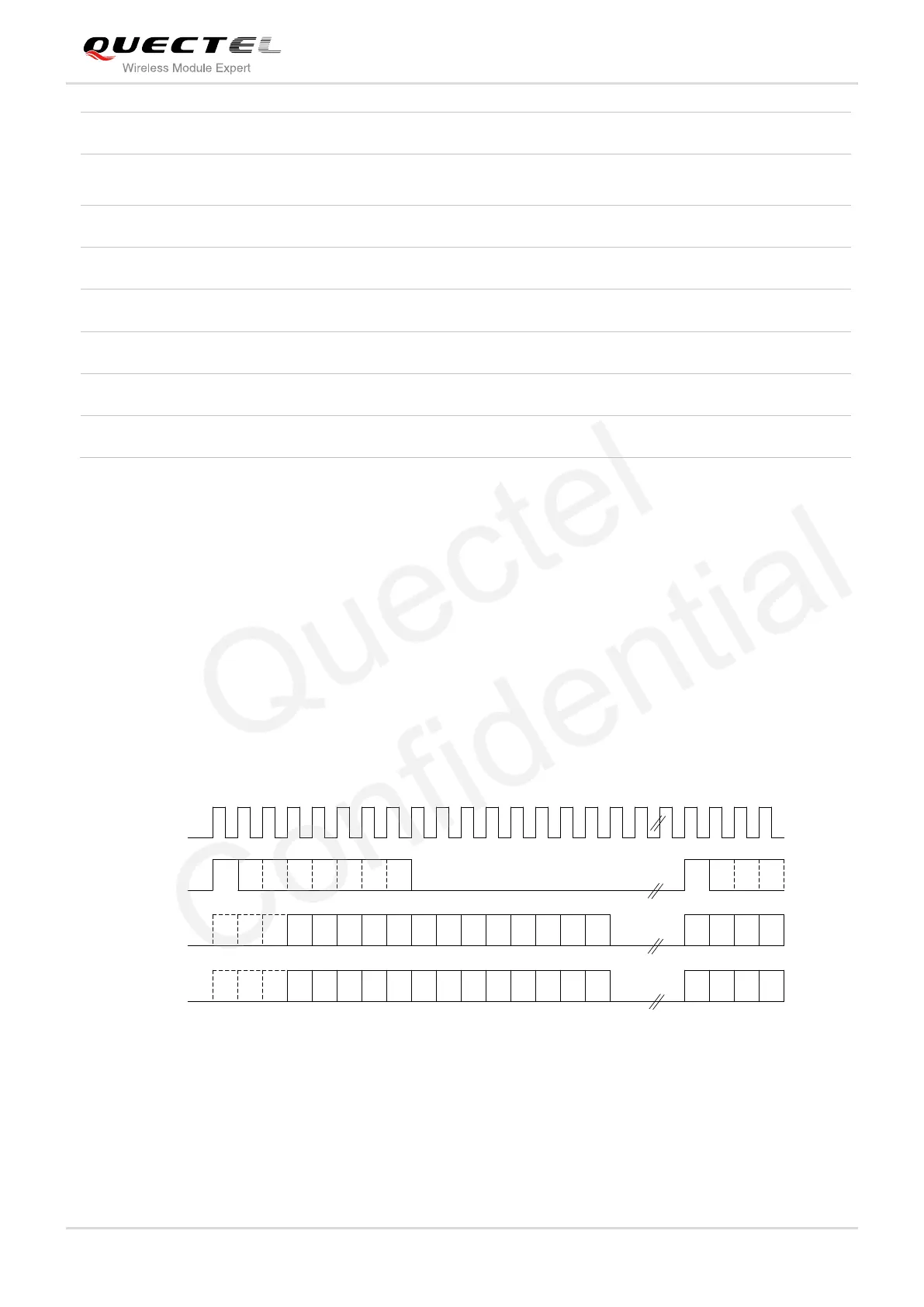
3.9.2. Timing
The sample rate of the PCM interface is 8 KHz and the clock source is 256 KHz, so every frame contains
32 bits data, since M66 supports 16 bits line code PCM format, the left 16 bits are invalid. The following
diagram shows the timing of different combinations. The synchronization length in long synchronization
format can be programmed by firmware from one bit to eight bits. In the Sign extension mode, the high
three bits of 16 bits are sign extension, and in the Zero padding mode, the low three bits of 16 bits are
zero padding.
Under zero padding mode, you can configure the PCM input and output volume by executing
AT+QPCMVOL command. For more details, please refer to Chapter 3.9.4.
12 11 10
9 8 7 6 5 4 3 2 1 0
12 11 10 9 8 7 6 5 4 3 2 1 0
PCM_CLK
PCM_SYNC
PCM_OUT
PCM_IN
MSB
MSB
Sign
extension
Sign
extension
Figure 28: Long Synchronization & Sign Extension Diagram
PCM Clock/Synchronization Source
PCM master mode: clock and synchronization is
generated by module
PCM master mode: 256 KHz (line)
PCM Synchronization Format
Long/short synchronization

 Loading...