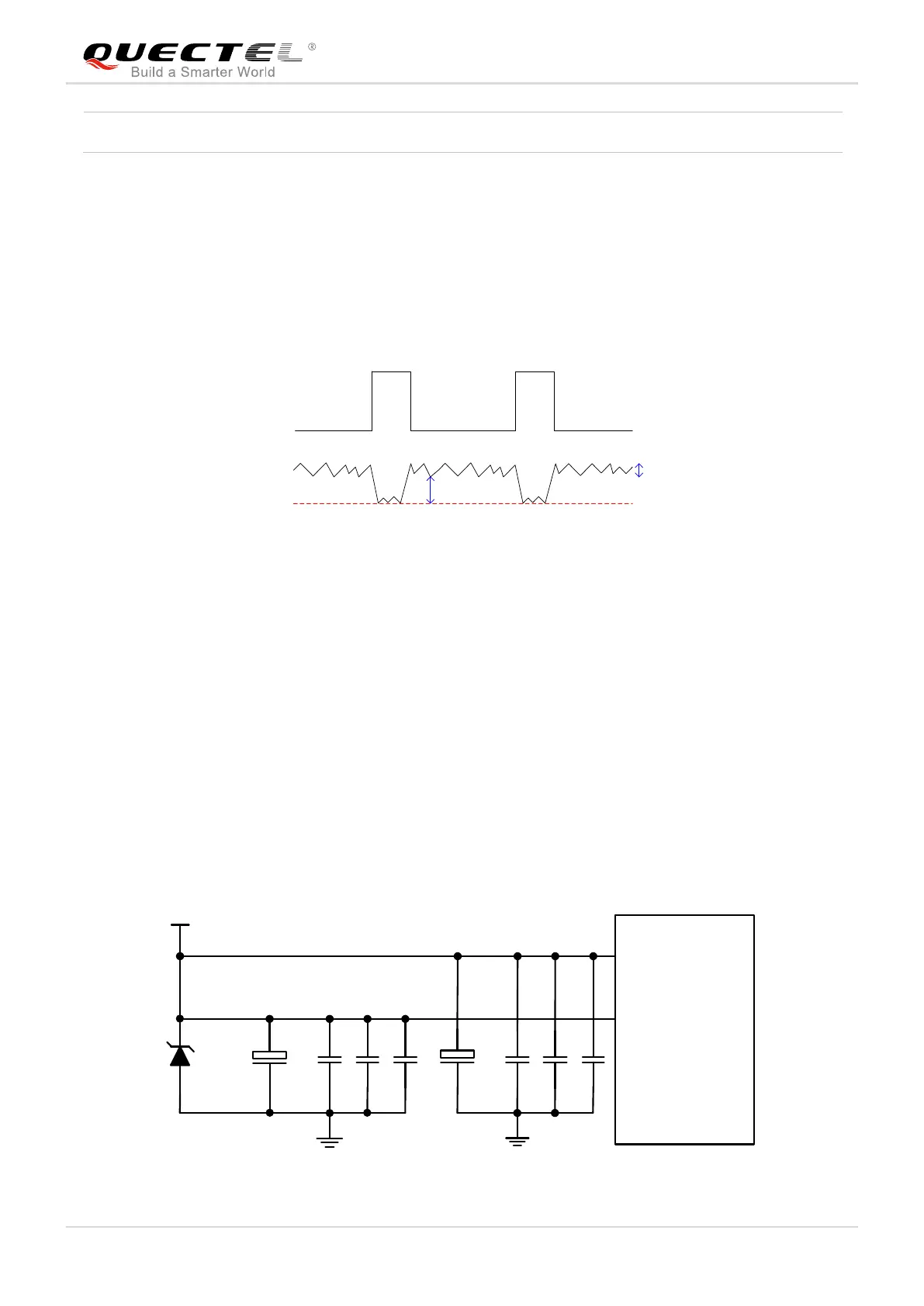
3.6.2. Decrease Voltage Drop
The power supply range of the module is from 3.3V to 4.3V. Please make sure that the input voltage will
never drop below 3.3V. The following figure shows the voltage drop during burst transmission in 2G
network. The voltage drop will be less in 3G and 4G networks.
Figure 7: Power Supply Limits during Burst Transmission
To decrease voltage drop, a bypass capacitor of about 100µF with low ESR (ESR=0.7Ω) should be used,
and a multi-layer ceramic chip (MLCC) capacitor array should also be reserved due to its ultra-low ESR. It
is recommended to use three ceramic capacitors (100nF, 33pF, 10pF) for composing the MLCC array,
and place these capacitors close to VBAT_BB/VBAT_RF pins. The main power supply from an external
application has to be a single voltage source and can be expanded to two sub paths with star structure.
The width of VBAT_BB trace should be no less than 1mm; and the width of VBAT_RF trace should be no
less than 2mm. In principle, the longer the VBAT trace is, the wider it will be.
In addition, in order to avoid the damage caused by electric surge and ESD, it is suggested that a TVS
diode such as WS4.5D3HV with low reverse stand-off voltage V
RWM
, low clamping voltage V
C
and high
reverse peak pulse current I
PP
should be used. The following figure shows the star structure of the power
supply.

 Loading...