Renesas RA Microcontrollers EK-RA4M1 v1 – User's Manual
R20UT4579EU0100 Rev.1.00 Page 15 of 32
Oct.02.19
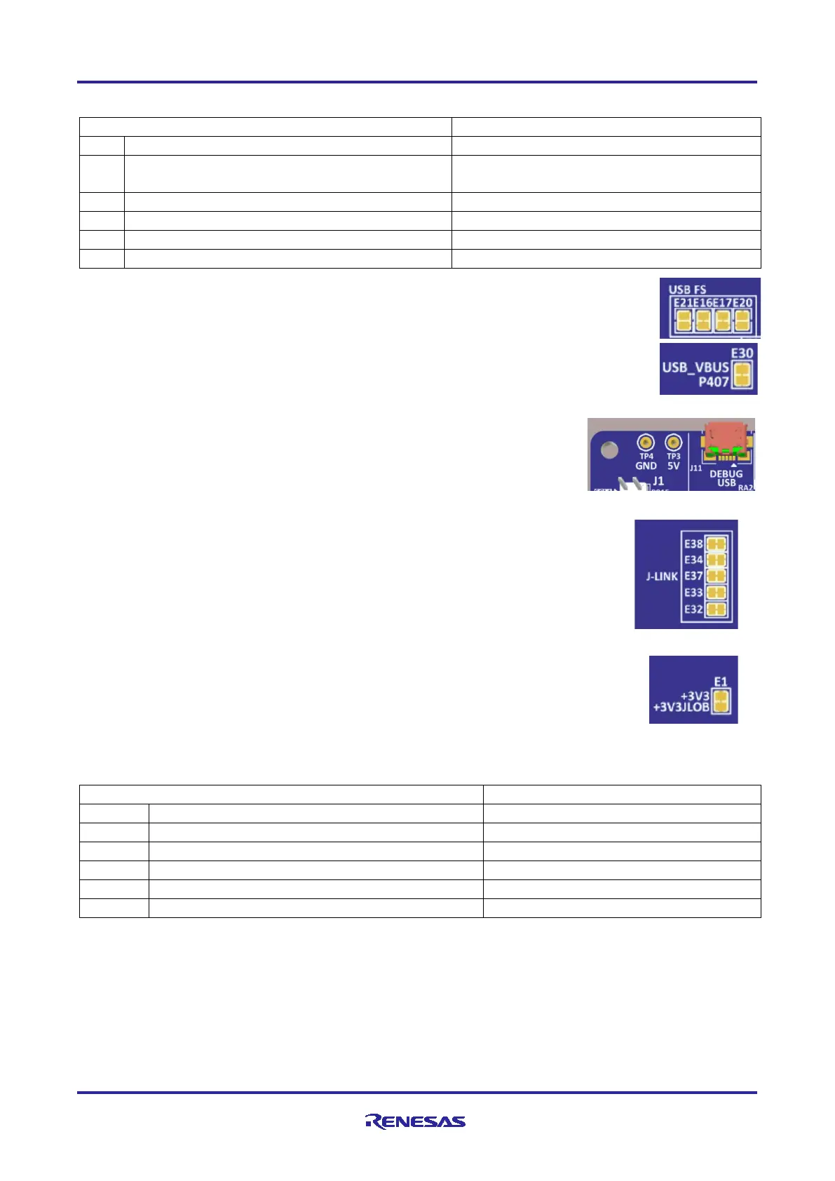
Table 2. DEVICE USB Connector (J9)
+5VDC, connected to a sense voltage 2/3 divider
to allow Main MCU sensing of Host presence
P407/USB_VBUS = 2/3(5VUSB)
USB ID, jack internal switch, cable inserted
Connections in Table 2 are based on the condition of copper jumpers E16, E17, E20, E21,
and E30 matching their as-manufactured status. As manufactured, E16 and E17 are
closed, E20 and E21 are open, and E30 is closed.
Alternatively, the Device USB signals to the Main MCU may be connected to MCU Pin
Header J1. To enable this configuration, copper jumpers E16 and E17 should be open, E20
and E21 should be closed.
5.4.2 Debug USB
The DEBUG USB Micro-B connection jack connects the S124 J-Link MCU to
an external USB Host, FS capable, allowing re-programming and debugging of
the Main MCU firmware. Power for the board may be received from this
connector.
The J-Link
®
OB interface is multiplexed with the JTAG interface, and can collectively be
referred to as the Programming Interface. While the J-Link
®
OB interface and the JTAG
interface do not conflict, the J-Link
®
OB signals may be isolated from the programming
interface by changing the associated copper jumpers.
J-Link Disconnect Copper Jumpers E32, E33, E34, E37, and E38, connect the J-Link
signals to the MCU programming interface. To isolate the J-Link signals from the JTAG
interface, the copper jumpers must be open. To allow use of the J-Link interface, each
copper jumper must be closed.
J-Link MCU Power Copper Jumper, E1, connects the main +3.3 V power to the J-Link
+3.3 V power. The default condition for E1 is closed, which connects the J-Link MCU
power to the main +3.3 V power. If J-Link signals are disconnected, the power to the
J-Link MCU should also be removed by changing E1 to open.
Table 3. DEBUG USB Connector (J11)
USB ID, jack internal switch, cable inserted
Three of the J-Link ports (P108, P109, and P300) are multiplexed with the SPI Fixed Pin function on pin
header J1. To use these signals for the SPI function, the J-Link debug function must be disabled. Details of
the multiplexed signals are shown in the following table.
 Loading...