Renesas RA Microcontrollers EK-RA4M1 v1 – User's Manual
R20UT4579EU0100 Rev.1.00 Page 3 of 32
Oct.02.19
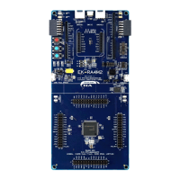
1. Kit Overview
The EK-RA4M1 v1 enables developers to get started with initial firmware development.
• Renesas RA4M1 Microcontroller Group
R7FA4M1AB3CFP
100-pin LQFP package
48 MHz Arm
®
Cortex
®
-M4 core with Floating Point Unit (FPU)
32 KB SRAM
256 KB code flash memory
8 KB data flash memory
• Connectivity
A Device USB connector for the Main MCU
SEGGER J-Link
®
On-Board (OB) interface for debugging and programming of the RA4M1 MCU. A
10pin JTAG/SWD interface is also provided for connecting optional external debuggers and
programmers.
Two PMOD connectors, allowing use of appropriate PMOD compliant peripheral plug-in modules for
rapid prototyping
Pin headers for access to power and signals for the Main MCU
• Multiple clock sources
Main MCU oscillator crystals, providing precision 12.000 MHz and 32,768 Hz external reference
clocks
Additional low-precision clocks are available internal to the Main MCU
• MCU reset push-button switch
• MCU boot configuration jumper
• General purpose I/O ports
One jumper to allow measuring of Main MCU current
Copper jumpers on PCB bottom side for configuration and access to selected MCU signals
• Operating voltage
External 5 V input through the Debug USB connector supplies the on-board power regulator to power
the Evaluation Kit logic and interfaces. External 5 V or 3.3 V may also be supplied through alternate
locations on the Evaluation Kit.
• A two-color board status LED indicating availability of regulated power and connection status of the J-Link
interface
• A red User LED, controlled by the Main MCU firmware
• A User Push-Button switch, User Capacitive Touch Sensor (button), and an optional User Potentiometer,
all of which are controlled by the Main MCU firmware.
 Loading...