Renesas RA Microcontrollers EK-RA4M1 v1 – User's Manual
R20UT4579EU0100 Rev.1.00 Page 25 of 32
Oct.02.19
5.5.4 Pin Header J4
Pin Header J4 is a 2-column by 20-row through-hole pin header on 2.54 mm centers.
Table 15. Pin Header J4 Pin Assignment
Color Key
Secondary Fixed Function pins
5.6 Additional Features
5.6.1 Analog Reference Voltages
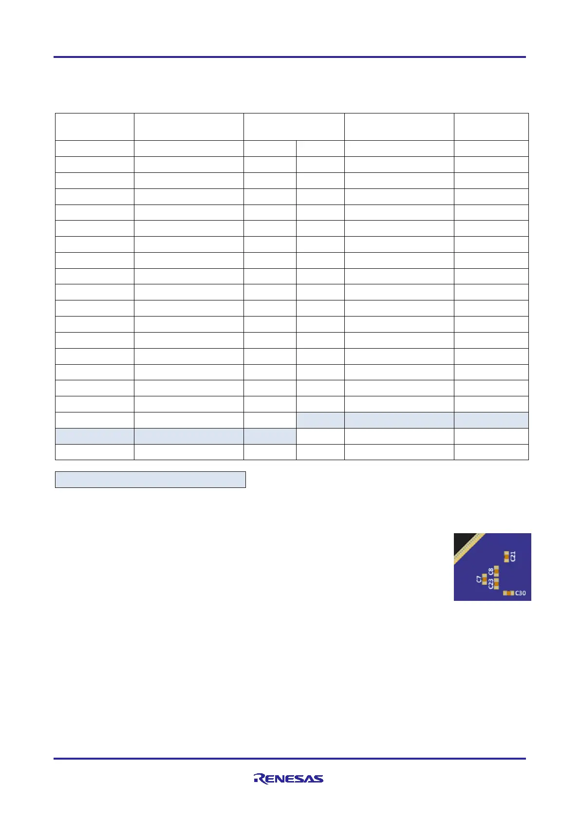
Footprints for the installation of capacitors C21 and C23 are provided on the board. These
two capacitors provide noise-bypass capability for ports P010/P011 and for ports
P012/P013. See Figure 24 for the circuit design.
Port pair P010/P011 may be assigned as GPIO, where bypass capacitor C21 would
damage signal quality. When P010/P011 are to be assigned as VREFH0/VREFL0,
installation of the capacitor C21 can reduce reference voltage noise and improve ADC
measurement and DAC output quality. The board was designed for Samsung P/N CL10B104KB8NNNC, or
similar, noise-bypass capacitors.
Port pair P012/P013 may be assigned as GPIO, where bypass capacitor C23 would damage signal quality.
When P012/P013 are to be assigned as VREFH/VREFL, installation of capacitor C23 may reduce reference
voltage noise and improve ADC measurement and DAC output quality. The board was designed for
Samsung P/N CL10B104KB8NNNC, or similar noise-bypass capacitors.
 Loading...