EasyManua.ls Logo

Renesas RL78/F24 User Manual

Renesas RL78/F24
58 pages
To Next Page IconTo Next Page
To Previous Page IconTo Previous Page
Page #42 background imageLoading...
Page #42 background image
E1/E20/E2/E2 Lite Additional Document 3. Notes on Usage
R20UT1994EJ0900 Rev.9.00 Page
42
of 58
Jan.20.22
3.3.2 Securing a Stack Area for Debugging
The debugger requires 4 bytes as a stack area for debugging except if start/stop functions (only supported
by the E2/E2 Lite) are in use, in which case the size of the stack area for debugging is up to 8 bytes. Since
this area is allocated immediately below the main stack area, the address of this area varies with increases
and decreases in the stack size. That is, if a program is using none of the stack (the stack is empty), the 4- or
8-byte stack area for the debugger remains.
Make sure the stack area for debugging does not go beyond the range of the internal RAM space.*
1
When a monitoring point (extended function of the E2) is in use, the size of the stack area for debugging is 6
bytes.
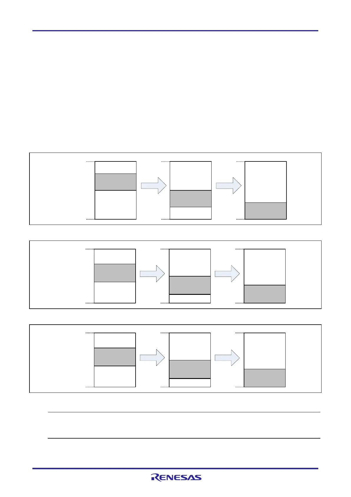
Figure 3-3 to Figure 3-5 show examples in which the stack area has increased with the start address of the
internal RAM space being 0xFCF00.
Stack area for
debugging
4 bytes or 12 bytes
Stack area
Available space
in internal RAM
0xFCF00
0xFFEDF
Stack area for
debugging
4 bytes or 12 bytes
Stack area
Available space
in internal RAM
0xFCF00
0xFFEDF
Stack area for
debugging
4 bytes or 12 bytes
Stack area
0xFFEDF
0xFCF00
Figure 3-3 Variation of Address of Stack Area for Debugging (E1/E20)
Stack area
Available space
in internal RAM
0xFCF00
Stack area for
debugging
4 bytes, 8 bytes, or
12 bytes
0xFFEDF
Stack area
Available space
in internal RAM
0xFCF00
0xFFEDF
Stack area
0xFCF00
0xFFEDF
Stack area for
debugging
4 bytes, 8 bytes, or
12 bytes
Stack area for
debugging
4 bytes, 8 bytes, or
12 bytes
Figure 3-4 Variation of Address of Stack Area for Debugging (E2 Lite)
Stack area
Available space
in internal RAM
0xFCF00
Stack area for
debugging
4 bytes, 6 bytes,
8 bytes, or 12 bytes
0xFFEDF
Stack area
Available space
in internal RAM
0xFCF00
0xFFEDF
Stack area
0xFCF00
0xFFEDF
Stack area for
debugging
4 bytes, 6 bytes,
8 bytes, or 12 bytes
Stack area for
debugging
4 bytes, 6 bytes,
8 bytes, or 12 bytes
Figure 3-5 Variation of Address of Stack Area for Debugging (E2)
*1
During self-programming, the size of the stack area for debugging is up to 12 bytes.
Refer to the self-programming manual for how to secure the stack area for self programming.
The start/stop function is disabled for self-programming.

Table of Contents

Question and Answer IconNeed help?

Do you have a question about the Renesas RL78/F24 and is the answer not in the manual?

Renesas RL78/F24 Specifications

General IconGeneral
BrandRenesas
ModelRL78/F24
CategoryComputer Hardware
LanguageEnglish

Summary

General Precautions in the Handling of Microprocessing Unit and Microcontroller Unit Products

Overview

Overview of E1/E20/E2 Emulator and E2 emulator Lite

Introduces the E1, E20, E2, and E2 Lite as on-chip debugging emulators for Renesas MCUs.

Supported Devices

Lists the RL78 family MCUs compatible with the emulators.

Overview of the Specifications of the External Trigger Input and Output

Details the external trigger functionality of the E2 emulator.

Terminology

Designing the User System

Connecting the E1/E20/E2/E2 Lite to the User System

Explains the initial connection requirements for the user system.

Installing the Connector on the User System

Covers the physical installation of connectors and adapters for system integration.

Pin Assignments of the Connector on the User System

Details the specific pin configurations of the emulator's 14-pin connector.

Recommended Circuits between the Connector and the MCU

Provides essential circuit diagrams for connecting the emulator to various RL78 MCUs.

Notes on Connection

Offers critical guidelines and precautions for signal connections.

Internal Circuits of the Emulator

Illustrates the internal circuitry of the emulators.

Notes on Designing the User System

Additional design considerations, including isolators and connector adapters.

Notes on Usage

Turning the Power On/Off

Step-by-step procedures for safe power management of the emulator and user system.

MCU Resources to be Occupied

Identifies memory areas used by the emulator for debugging operations.

Setting a Security ID

Covers setting security IDs to prevent unauthorized access and enable debugging.

Reset

Discusses reset behavior and its impact on debugging processes.

Flash Memory

Addresses specific considerations for flash memory programming.

MCUs that are Used in Debugging

Advises on proper handling of MCUs used during the debugging phase.

Final Evaluation of the User Program

Emphasizes pre-production evaluation without the emulator.

Debug Functions

Provides an overview of the various debugging features available.

Stepped Execution

Explains stepped execution and associated considerations.

Pseudo-Real-Time RAM Monitor Function or Pseudo-Dynamic Memory Modification Function

Notes on using pseudo-RRM/DMM functions, including clock dependencies.

Points for Caution on Using the RL78/G23

Highlights precautions specific to the RL78/G23, such as flash read protection.

Points for Caution on Using the RL78/F24

Covers critical cautions for the RL78/F24, including security and reset handling.

Revision History

Related product manuals