• Low-cost QFP and BGA packaging options
- Common footprints support easy density migration
- Pb-free packaging options
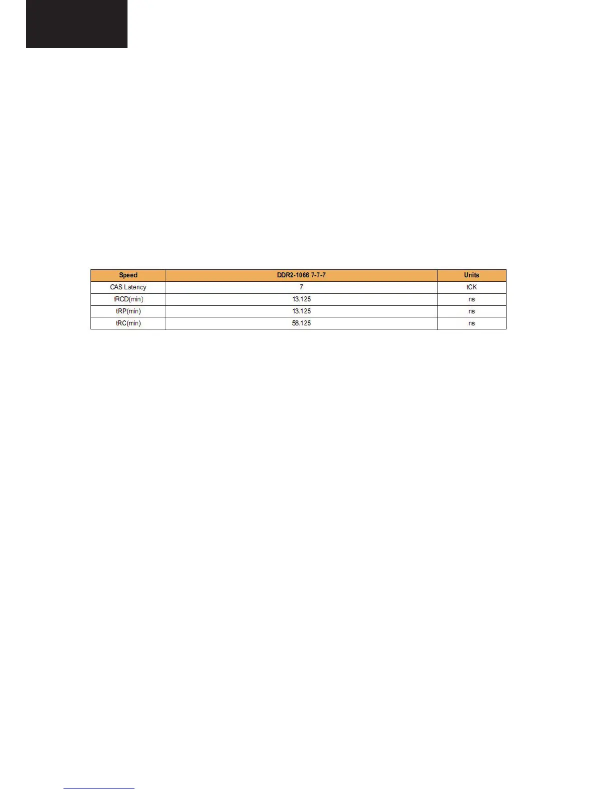
8. 1Gb F-die DDR2-1066 SDRAM (U41-U42-U8-U9)
Samsung K4T1G084QF
a) Key Features
• JEDEC standard VDD = 1.8V ± 0.1V Power Supply
•VDDQ = 1.8V ± 0.1V
• 533MHz fCK for 1066Mb/sec/pin
• 8 Banks
• Posted CAS
• Programmable CAS Latency: 4, 5, 6, 7
• Programmable Additive Latency: 3, 4, 5. 6
• Write Latency(WL) = Read Latency(RL) -1
• Burst Length: 4 , 8(Interleave/nibble sequential)
• Programmable Sequential / Interleave Burst Mode
• Bi-directional Differential Data-Strobe (Single-ended data-strobe is an optional feature)
• Off-Chip Driver(OCD) Impedance Adjustment
• On Die Termination
• Special Function Support
- PASR(Partial Array Self Refresh)
- 50ohm ODT
- High Temperature Self-Refresh rate enable
• Average Refresh Period 7.8us at lower than TCASE 85°C, 3.9us at 85°C < TCASE < 95 °C
• All of products are Lead-free, Halogen-free, and RoHS compliant
The 1Gb DDR2 SDRAM is organized as a 16Mbit x 8 I/Os x 8 banks, 8Mbit x 16 I/Os x 8
banks device. This synchronous device achieves high speed double-data-rate transfer rates of
up to 1066Mb/sec/pin (DDR2-1066) for general applications.
The chip is designed to comply with the following key DDR2 SDRAM features such as
posted CAS with additive latency, write latency = read latency - 1, Off-Chip Driver(OCD)
impedance adjustment and On Die Termination. All of the control and address inputs are
synchronized with a pair of externally supplied differential clocks. Inputs are latched at the
crosspoint of differential clocks (CK rising and CK falling). All I/Os are synchronized with a
pair of bidirectional strobes (DQS and DQS) in a source synchronous fashion. The address
 Loading...