For Schematic Diagrams.
Note:
• All capacitors are in μF unless otherwise noted. (p: pF) 50
WV or less are not indicated except for electrolytics and
tantalums.
• All resistors are in Ω and 1/4 W or less unless otherwise
specifi ed.
•
f
: internal component.
• C : panel designation.
THIS NOTE IS COMMON FOR PRINTED WIRING BOARDS AND SCHEMATIC DIAGRAMS.
(In addition to this, the necessary note is printed in each block.)
• A : B+ Line.
• B : B– Line.
• Voltages and waveforms are dc with respect to ground
under no-signal (detuned) conditions.
– DMB-FIT Board –
no mark
: DVD PLAY
– Other Boards –
no mark
: TUNER (FM)
( ) : DVD PLAY
• Voltages are taken with VOM (Input impedance 10 MΩ).
Voltage variations may be noted due to normal production
tolerances.
• Waveforms are taken with a oscilloscope.
Voltage variations may be noted due to normal production
tolerances.
• Circled numbers refer to waveforms.
• Signal path.
J : CD PLAY
c : DVD PLAY
F : AUDIO
E : VIDEO
f : TUNER (FM)
N : MIC
P : USB
• Abbreviation
AUS : Australian model
CND :
Canadian model
E3 : 240V AC area in E model
E15 : Iranian model
E32 : Latin American model (110 – 240V AC area)
EA : Saudi Arabia model
KR : Korean model
MX : Mexican model
RU : Russian model
SP : Singapore model
TH : Thai model
TW : Taiwan model
For Printed Wiring Boards.
Note:
• X : Parts extracted from the component side.
• Y : parts extracted from the conductor side.
•
f
: internal component.
• : Pattern from the side which enables seeing.
(The other layers' patterns are not indicated.)
Caution:
Pattern face side:
(SIDE B)
Parts face side:
(SIDE A)
Parts on the pattern face side seen from
the pattern face are indicated.
Parts on the parts face side seen from
the parts face are indicated.
Note:
The components identi-
fi ed by mark 0 or dotted
line with mark 0 are criti-
cal for safety.
Replace only with part
number specifi ed.
Note:
Les composants identifi és
par une marque 0 sont
critiques pour la sécurité.
Ne les remplacer que par
une piéce portant le nu-
méro spécifi é.
Caution:
Pattern face side:
(Conductor Side)
Parts face side:
(Component Side)
Parts on the pattern face side seen from
the pattern face are indicated.
Parts on the parts face side seen from
the parts face are indicated.
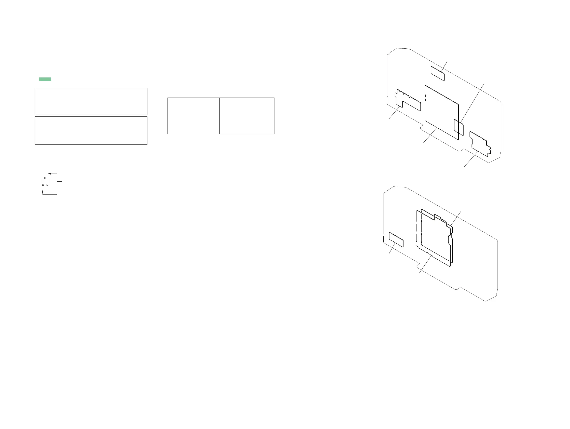
• DMB-FIT board is multi-layer printed board.
However, the patterns of intermediate layers have not
been included in diagrams.
• Indication of transistor.
These are omitted.
 Loading...