4-1
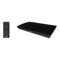
BDP-S7200
SECTION 4
PRINTED WIRING BOARDS
4-1.
THIS NOTE IS COMMON FOR PRINTED WIRING BOARDS
21
3
21
3
21
32
EB
C
3
55
22233 3
4
4
45
5111
1664 5
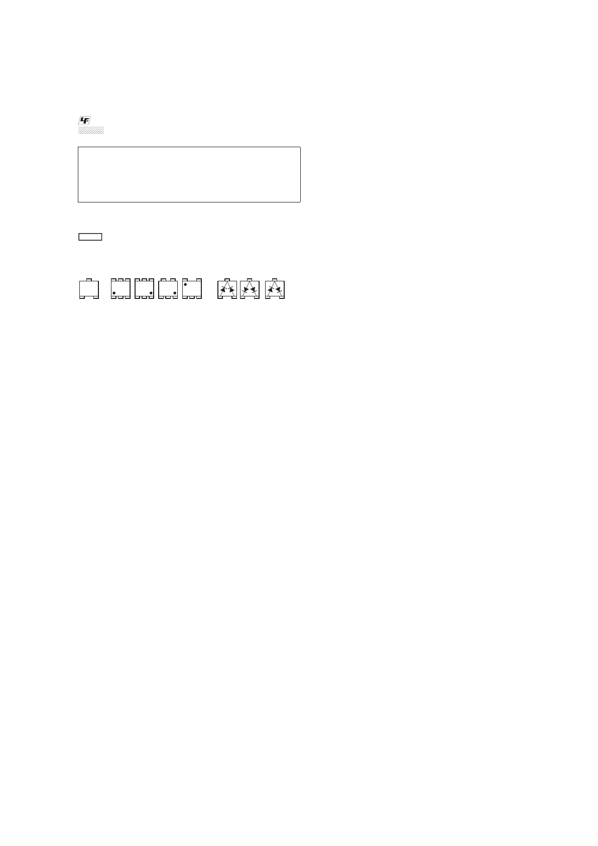
Transistor Diode
: Uses unleaded solders.
: Pattern from the side which enables seeing.
(The other layers’ patterns are not indicated)
Through hole is omitted.
There are few cases that the part printed on diagram isn’t mounted
in this model.
: panel designation
Chip parts.
Caution:
Pattern face side:
(SIDE B)
Parts face side:
(SIDE A)
Parts on the pattern face side seen from
the pattern face are indicated.
Parts on the parts face side seen from
the parts face are indicated.
 Loading...