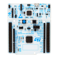
Hardware layout and configuration UM1724
38/68 UM1724 Rev 14
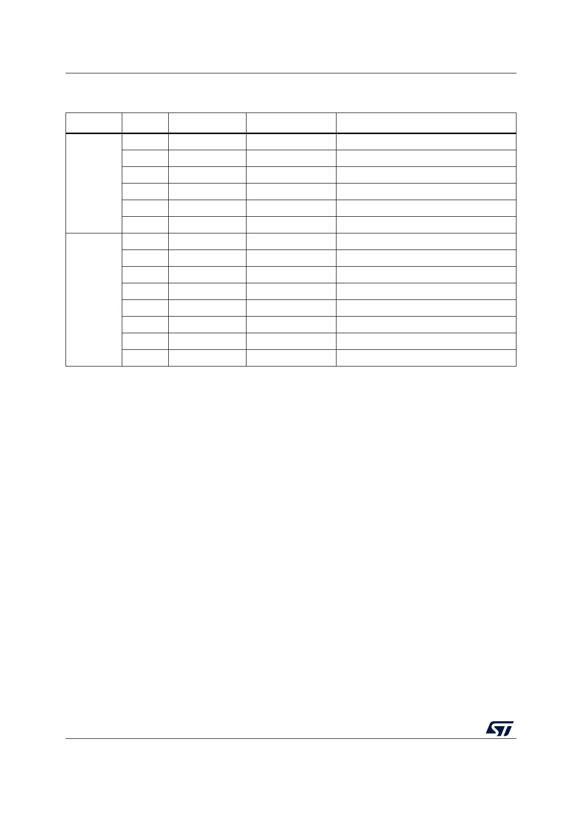
CN5 digital
6 D13 PA5 SPI1_SCK
5 D12 PA6 SPI1_MISO
4 D11 PA7 TIM17_CH1 or SPI1_MOSI
3 D10 PB6 TIM16_CH1N or SPI1_CS
2 D9 PC7 TIM3_CH2
1D8 PA9 -
CN9 digital
8D7 PA8 -
7 D6 PB10 TIM2_CH3
(2)
6 D5 PB4 TIM3_CH1
5 D4 PB5 -
4 D3 PB3 TIM2_CH2
(3)
3D2 PA10 -
2 D1 PA2 USART2_TX
1 D0 PA3 USART2_RX
1. Refer to Table 10: Solder bridges for details.
2. PWM is not supported by D6 on STM32F030 and STM32F070 since the timer is not available on PB10.
3. PWM is not supported by D3 on STM32F030 and STM32F070 since the timer is not available on PB3.
Table 11. ARDUINO
®
connectors on NUCLEO-F030R8, NUCLEO-F070RB,
NUCLEO-F072RB, NUCLEO-F091RC (continued)
Connector Pin Pin name STM32 pin Function
 Loading...