Hardware layout and configuration UM1724
60/68 UM1724 Rev 14
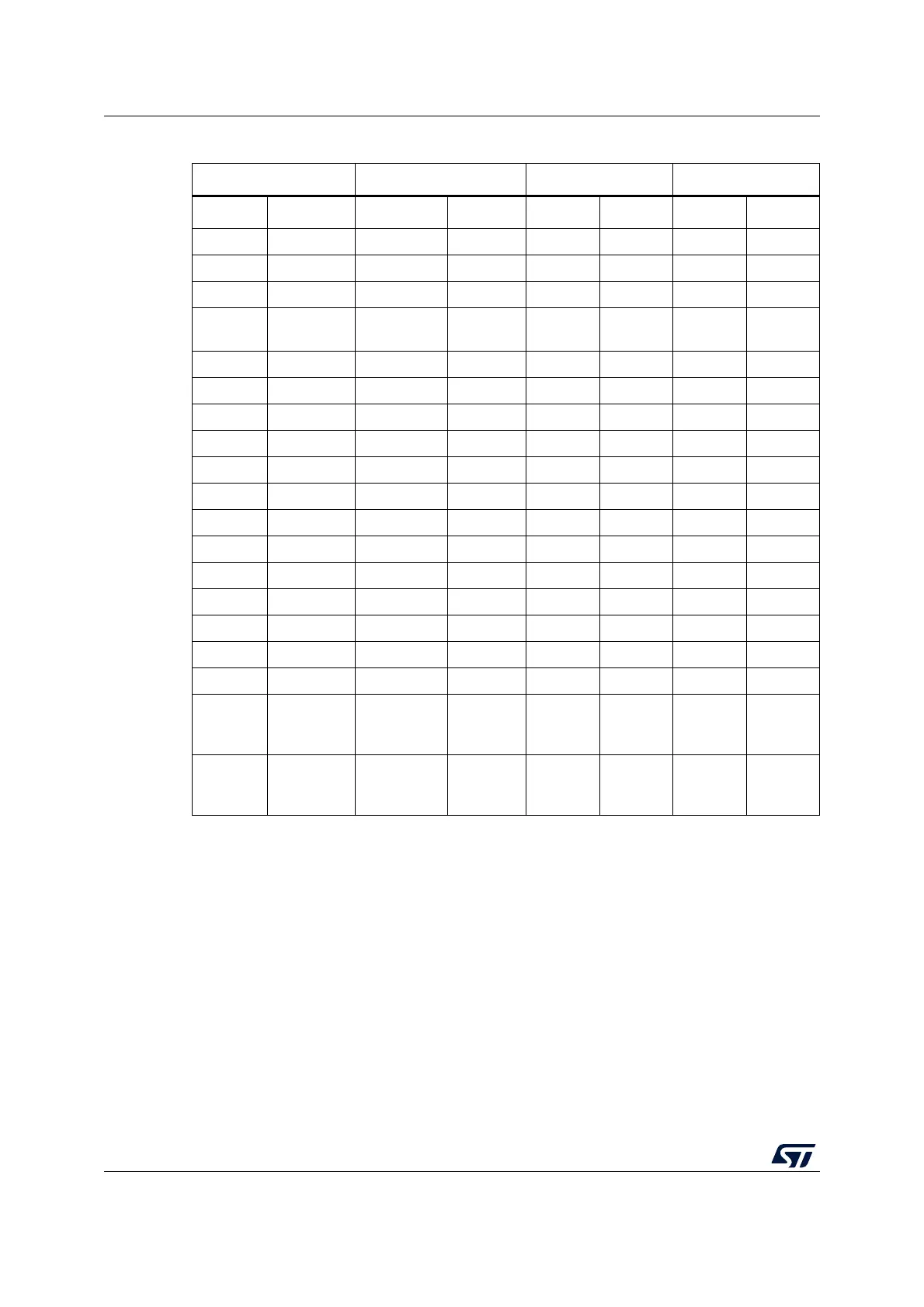
Table 31. ST morpho connector on NUCLEO-L452RE
CN7 odd pins CN7 even pins CN10 odd pins CN10 even pins
Pin Name Name Pin Pin Name Name Pin
1 PC10 PC11 2 1 PC9 PC8 2
3 PC12 PD2 4 3 PB8 PC6 4
5 VDD E5V 6 5 PB9 PC5 6
7
PH3 /
BOOT0
(1)
1. The default state of BOOT0 is LOW. It can be set to HIGH when a jumper is on pins 5-7 of CN7.
GND 8 7 AVDD U5V
(2)
2. U5V is 5 V power from ST-LINK/V2-1 USB connector and it rises before +5V.
8
9- -109GND-10
11 - IOREF 12 11 PA5 PA12 12
13 PA13
(3)
3. PA13 and PA14 share with SWD signals connected to ST-LINK/V2-1, it is not recommended to
use them as IO pins if the ST-LINK part is not cut.
RESET 14 13 PA6 PA11 14
15 PA14
(3)
+3.3V 16 15 PA7 PB12 16
17 PA15 +5V 18 17 PB6 PB11 18
19 GND GND 20 19 PC7 GND 20
21 PB7 GND 22 21 PA9 PB2 22
23 PC13 VIN 24 23 PA8 PB1 24
25 PC14 - 26 25 PB10 PB15 26
27 PC15 PA0 28 27 PB4 PB14 28
29 PH0 PA1 30 29 PB5 PB13 30
31 PH1 PA4 32 31 PB3 AGND 32
33 VBAT PB0 34 33 PA10 PC4 34
35 PC2
PC1
or
PB9
(4)
4. Refer to Table 10: Solder bridges for details.
36 35 PA2 - 36
37 PC3
PC0
or
PB8
(4)
38 37 PA3 - 38
 Loading...