Recommended PCB routing guidelines for STM32F4xxxx devices AN4488
42/50 AN4488 Rev 7
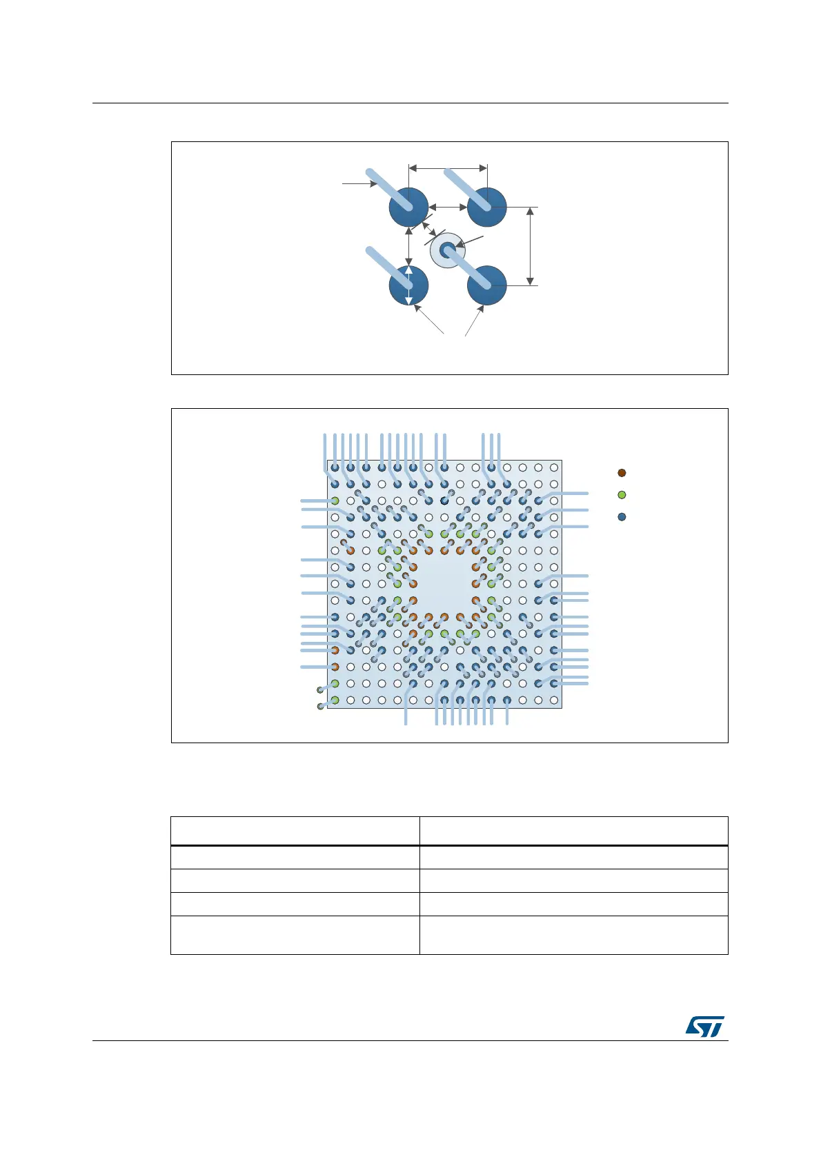
Figure 25. Via fan-out
Figure 26. FMC signal fan-out routing example
8.5.2 WLCSP143 0.4 mm pitch design example
06Y9
PP
PP
PP
PP
6XUIDFH/DQG3DG
PP
3DG
9LD
9LD'ULOO
3DGWRYLD
VSDFH
7UDFH
06Y9
$
%
&
'
(
)
*
+
-
.
/
0
1
3
5
3:5
*1'
)0&
Table 10. Wafer level chip scale package information
Package information (mm) Design parameters (mm)
Bump pitch : 0.4 Microvia size : hole size ∅= 0.1, via land: 0.2
Bump size : 0.25 Trace width/space : 0.07/0.05 or 0.07/0.07
Number of rows/columns : 13x11 Bump pad size ∅= 0.26 max – 0.22 recommended
Non-solder mask defined via underbump
allowed
Solder mask opening bump ∅=0.3 min (for 0.26
diameter pad)
 Loading...


