AN4488 Rev 7 41/50
AN4488 Recommended PCB routing guidelines for STM32F4xxxx devices
49
8.5 Package layout recommendation
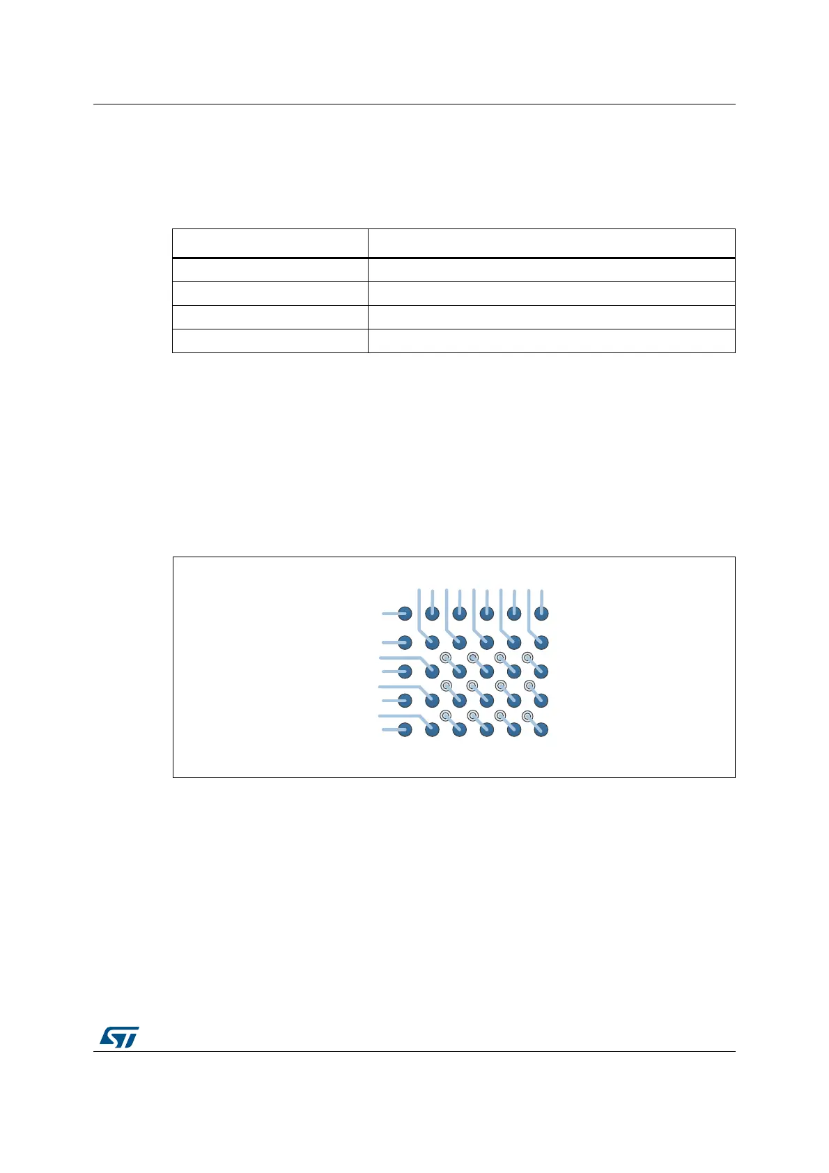
8.5.1 BGA 216 0.8 mm pitch design example
With 0.8 mm pitch BGA balls, fan-out vias are needed to route the balls to other layers on
the PCB. Through-vias are used in this example, which cost less than blind, buried vias. For
four adjacent BGA land pads, it is possible to have only one via as showing in
Figure 24 and
Figure 25. The traces are routed of two first row and two first colon without fan-out via. The
current pitch size allows to route only one trace between two adjacent BGA land pads.
Figure 26 shows an example of ideal SDRAM signals fan-out vias with power and gnd
signals. These signals can be optimized to achieve the routing and length matching in an
another layer before connecting to an SDRAM IC.
Figure 24. BGA 0.8mm pitch example of fan-out
Table 9. BGA 216 0.8 mm pitch package information
Package information (mm) Design parameters (mm)
Ball pitch : 0.8 Via size : hole size ∅= 0.2, pad size: 0.45, plane clearance: 0.65
Ball size : 0.4 Trace width : 0.10/0.125
Number of rows/columns : 15x15 Trace/trace space : 0.10/0.125
Package solder Pad: SMD BGA land size (Ball pad): ∅= 0.4, solder mask: 0.5
 Loading...