Maintenance
TDS1000 and TDS2000 Series Digital Storage Oscilloscopes Service Manual
6-- 37
exploded diagrams in Replaceable Parts for the location and orientation of
the connector on the main board.
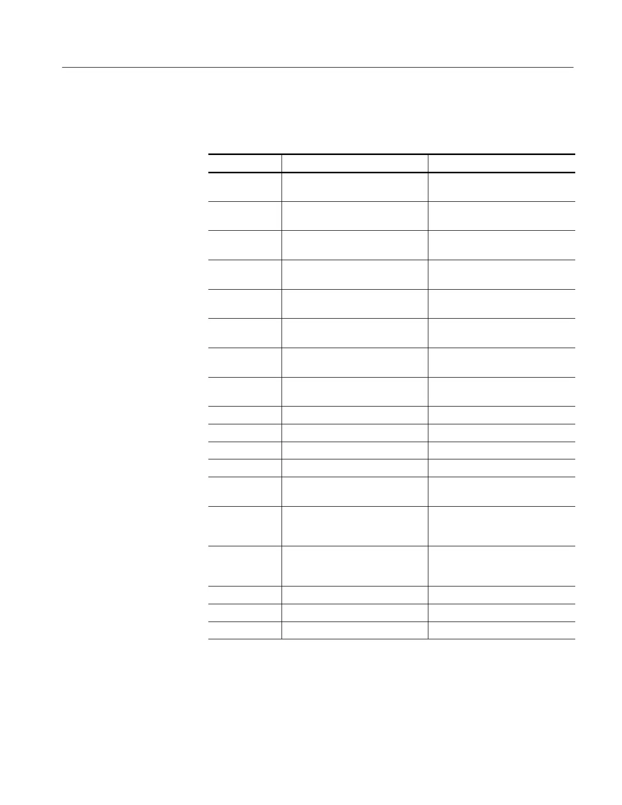
Signal at J201 Description, Monochrome Description, Color
Pin 1 (marked
with
A )
No fixed pattern. Depends upon
display data.
No fixed pattern. Depends upon
display data.
Pin 2 No fixed pattern. Depends upon
display data.
No fixed pattern. Depends upon
display data.
Pin 3 No fixed pattern. Depends upon
display data.
No fixed pattern. Depends upon
display data.
Pin 4 No fixed pattern. Depends upon
display data.
No fixed pattern. Depends upon
display data.
Pin 5 Not connected No fixed pattern. Depends upon
display data.
Pin 6 Not connected No fixed pattern. Depends upon
display data.
Pin 7 Not connected No fixed pattern. Depends upon
display data.
Pin 8 Not connected No fixed pattern. Depends upon
display data.
Pin 9 24 V
DC
2
26.5 V
DC
2
Pin 10 Ground Ground
Pin 11 +5 V
DC
+5 V
DC
Pin 12 HI when display active HI when display active
Pin 13 Data rate clock.
1.36 MHz Square wave
3
Data rate clock.
1.36 MHz Square wave
Pin 14 Line rate clock
17 kHz, 500 ns high pulse from low
baseline
3
Line rate clock
11.4 kHz, 500 ns high pulse from low
baseline
Pin 15 Frame rate clock
70 Hz, 750 ns high pulse from low
baseline
3
Frame rate clock
43 Hz, 350 ns high pulse from low
baseline
Pin 16 Low
4
High (> 2.4 V)
Pin 17 Ground Ground
Pin 18 Ground Ground
2
Value varies with temperature, contrast setting, and display type.
3
Frequency may vary slightly with software version.
4
With monochrome display cable attached. If no cable is attached, default condition is
High (color).
 Loading...