Specifications
Table 6: Typical electrical characteristics (cont.)
Characteristic Description
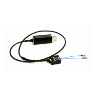
TekFlex solder-in tips P77BRWSR
Channel isolation Unfiltered probe tip and typical probe response
50 MHz <40 dB N.A.
1GHz
<30 dB N.A.
10 GHz
<15 dB N.A.
20 GHz
<6 dB N.A.
Output zero
temperature drift
Voltage measured at probe output
±100 μV/°C, from -35 °C to +85 °C (-31 °F
to +185 °F)
±100 μV/°C, from 0 °C to +45 ° C
(+32 °F to +113 °F)
Noise, analog (all Input
modes)
Offset voltage range
-4Vto+4V -10Vto+10V
Small signal frequency
response
2
DSP corrected, probe tip and typical probe response
Differential, A, B, and Common mode
P7720
≥20 GHz ≥16 GHz
P7716
≥16 GHz ≥16 GHz
P7713
≥13 GHz
P7708
≥8GHz
Auto offset accuracy
Vin ±30 mV
Offset voltage gain
accuracy, probe and
probe tips
± 0.5% , A and B inputs, all step gain settings
DC voltage measurement accuracy (referred to input), including major error terms
4X, ABCD: ±(2% of input + 0.5% of offset + 11.4 mV + 3.8 mV) ±(2% of input + 0.5% of offset + 27.0 mV + 8.9 mV)
2X, ABCD: ±(2% of input + 0.5% of offset + 22.8 mV + 7.5 mV) ±(2% of input + 0.5% of offset + 53.9 mV + 17.8 m V)
1X, ABC: ±(2% of input + 0.5% of offset + 44.5 mV + 12.5 mV) ±(2% of input + 0.5% of offset + 107.9 m V + 30.0 mV)
1X, D:
±(2% of input + 0.5% of offset + 44.5 mV + 15.1 mV) ±(2% of input + 0.5% of offset + 107.9 mV + 35.7 mV)
½X, D: ±(2% of input + 0.5% of offset + 91.0 mV + 25.0 mV) ±(2% of input + 0.5% of offset + 215.7 mV + 60.0 mV)
Nondestructive input
voltage range,
A and B inputs
-15Vto+15V(DC+peakAC),tipattached
Time delay
P77xx 5.5 ns ±0.1 ns
P77STFLXA
260 ps ±10 ps
P77STCABL
515 ps ±10 ps
P77BRWSR
260 ps ±10 ps
Input slew rate
≥30 V/ns, single-ended, both inputs
P7700 Series TriMode Probes Technical Reference 41
 Loading...